Introduction
In the ever-evolving world of thin film technology, the precise control over material properties has become a defining factor in the success of semiconductor devices, optical coatings, solar cells, and beyond. Among the key enablers of these advancements are sputtering targets, which serve as the foundational source materials in physical vapor deposition (PVD) techniques. Among the many classes of sputtering targets available today, oxides, nitrides, and silicides occupy a crucial place—each delivering unique functional advantages tailored to specific application domains.
Understanding the performance differences between oxide, nitride, and silicide sputtering targets is essential not only for selecting the right material but also for achieving the desired film characteristics such as conductivity, hardness, optical transparency, and chemical stability. This article delves deep into their individual properties, comparative advantages, limitations, and real-world applications, giving scientists and engineers a clear path toward informed material choices.
The Nature of Sputtering Targets: A Quick Refresher
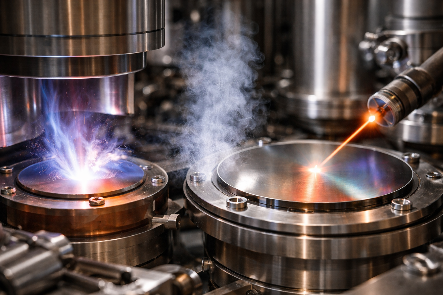
Before contrasting the categories, it’s important to revisit the core concept. A sputtering target is the solid material from which atoms are ejected under bombardment by energetic particles (typically argon ions) in a vacuum chamber. These atoms then condense onto a substrate, forming a thin film.
The behavior of the deposited film is largely influenced by the chemical and physical nature of the target. Oxide, nitride, and silicide targets differ significantly in:
- Bond structure
- Electrical properties
- Chemical reactivity
- Sputter yield and uniformity
- Thermal behavior
Oxide Sputtering Targets: Versatility in Functionality
Composition and Characteristics
Oxide sputtering targets are derived from metal-oxygen compounds, such as:
- ITO (Indium Tin Oxide)
- ZnO (Zinc Oxide)
- Al₂O₃ (Aluminum Oxide)
- TiO₂ (Titanium Dioxide)
- SiO₂ (Silicon Dioxide)
Oxides are generally insulating or semiconducting, often chosen for their optical transparency, chemical inertness, and dielectric properties. They can be fabricated through hot pressing, sintering, or ceramic bonding, and often exhibit low sputter rates, especially in reactive sputtering setups.
Applications
- Transparent Conductive Films:
ITO is widely used in touch screens, OLEDs, and solar cells due to its combination of conductivity and transparency. - Dielectric Layers:
SiO₂ and Al₂O₃ are essential in CMOS processes for gate insulation and surface passivation. - Optical Coatings:
Oxides like TiO₂ and ZrO₂ serve in anti-reflective coatings and beam splitters due to their adjustable refractive indices.
Strengths and Limitations
| Strengths | Limitations |
|---|---|
| Excellent chemical stability | Lower deposition rates |
| High optical transmission | Brittle target structure |
| Compatible with reactive sputtering | Moisture sensitivity (in some cases) |
Nitride Sputtering Targets: Hardness Meets Stability
Composition and Characteristics
Nitride targets consist of metal-nitrogen compounds, such as:
- TiN (Titanium Nitride)
- AlN (Aluminum Nitride)
- Si₃N₄ (Silicon Nitride)
- CrN (Chromium Nitride)
These materials are typically hard, chemically resistant, and thermally conductive. Their inherent metallic or semiconducting behavior makes them useful across a range of electronic and mechanical applications. Nitride targets are often ceramic in nature and require careful sintering and densification to achieve usable sputtering yields.
Applications
- Hard Coatings:
TiN is extensively used in cutting tools, wear-resistant coatings, and automotive parts. - Dielectric Films:
AlN offers high thermal conductivity and electrical insulation, ideal for RF devices and heat spreaders.- Passivation and Diffusion Barriers:
Si₃N₄ serves as a critical barrier layer in semiconductors, preventing metal diffusion and offering chemical protection.
Strengths and Limitations
| Strengths | Limitations |
|---|---|
| Exceptional mechanical hardness | Difficult target fabrication |
| High thermal stability | Lower sputter efficiency |
| Good chemical resistance | Brittle and fragile structure |
Silicide Sputtering Targets: Engineering Interconnectivity
Composition and Characteristics
Silicide sputtering targets are binary or ternary compounds of silicon with transition metals, including:
- MoSi₂ (Molybdenum Disilicide)
- TiSi₂ (Titanium Disilicide)
- CoSi₂ (Cobalt Silicide)
- NiSi (Nickel Silicide)
These materials are notable for their metal-like conductivity, oxidation resistance, and excellent compatibility with silicon-based semiconductor devices. Silicides are typically fabricated through arc melting, powder metallurgy, or hot pressing.
Applications
- Semiconductor Contacts:
TiSi₂ and NiSi are widely used in shallow junctions and gate contacts for CMOS technologies due to their low resistivity and silicon integration. - Resistive Heaters:
MoSi₂’s high oxidation resistance and thermal conductivity make it a choice material in furnace heaters. - Thermoelectric Devices:
Some silicides are being explored in high-temperature thermoelectric generators.
Strengths and Limitations
| Strengths | Limitations |
|---|---|
| Good electrical conductivity | Sensitive to phase segregation |
| Stable in silicon environments | Oxidation-prone at intermediate temperatures |
| Compatible with high-aspect-ratio features | Limited commercial availability (some types) |
Comparative Performance in Deposition Processes
| Property | Oxides | Nitrides | Silicides |
|---|---|---|---|
| Electrical Conductivity | Low to Moderate | Low to Moderate | High |
| Optical Transparency | High | Low | Opaque |
| Hardness | Moderate | Very High | Moderate |
| Thermal Stability | High | High | Very High |
| Sputter Rate | Low to Medium | Low | Medium |
| Moisture Sensitivity | Moderate (e.g., ZnO) | Low | Low |
| Film Uniformity | Excellent | Good | Good |
| Surface Adhesion | Strong (on glass, polymers) | Strong (on metals, ceramics) | Excellent (on silicon) |
Trends in Industry Use
Semiconductor Manufacturing
The push toward miniaturization has demanded new solutions for gate dielectrics and contact metals. Silicides such as NiSi have become the standard for 22nm and 14nm CMOS nodes. Meanwhile, high-k oxides like HfO₂ and ZrO₂ are replacing traditional SiO₂ to overcome dielectric leakage.
Optoelectronics
Oxide targets, especially ITO and ZnO, are dominating the transparent electrode market. Their integration with flexible and organic substrates continues to expand in wearable electronics and smart displays.
Solar Cells
The rapid growth in thin film solar technology has led to increased use of materials like ZnO:Al, SiO₂, and TiO₂ as buffer layers and AR coatings. Nitrides like Si₃N₄ are also used for surface texturing in crystalline silicon PV.
Hard Coatings
In industries such as aerospace and tooling, nitrides remain unmatched in durability and performance. Emerging applications in MEMS (Micro-Electro-Mechanical Systems) are also beginning to explore nitride-based films for reliability.
Deposition Method Compatibility
All three target types can be used in various sputtering techniques, but some forms perform better in specific systems:
- DC Magnetron Sputtering: Ideal for conductive silicides and some nitrides
- RF Sputtering: Required for insulating oxides
- Reactive Sputtering: Converts metal targets into oxide/nitride films in the presence of O₂ or N₂ gases
- Pulsed DC Sputtering: Helps reduce arcing during nitride deposition
- High-Power Impulse Magnetron Sputtering (HiPIMS): Improves adhesion and density, increasingly used for silicides and nitrides
Choosing the Right Material for Your Application
When deciding between oxide, nitride, and silicide sputtering targets, consider the following factors:
- Film function: Optical layer? Barrier? Conductor?
- Substrate compatibility: Glass, polymer, silicon, ceramic?
- Required conductivity or transparency
- Thermal budget of the deposition process
- Post-deposition processing (e.g., annealing)
For example:
- Use Al₂O₃ or SiO₂ when transparency and dielectric strength are priorities
- Use TiN or AlN for wear resistance or thermal conductivity
- Use TiSi₂ or NiSi for metal-semiconductor contact formation in logic devices
Conclusion
Oxide, nitride, and silicide sputtering targets each serve distinct, mission-critical roles across a wide range of thin film applications. Understanding their compositional differences, process behaviors, and performance characteristics is key to selecting the optimal target for your deposition system.
As industries continue to demand higher performance materials, and as thin film requirements become more specialized, the strategic selection of sputtering targets will only grow in importance. Whether you’re aiming for a transparent electrode, a diffusion barrier, or an ultra-low-resistance contact, mastering the differences among these advanced ceramic and compound materials is vital.
For those seeking consistent supply, high purity, and custom configurations of oxide, nitride, and silicide targets, TFM (ThinFilmMaterials.com) offers a robust catalog designed for cutting-edge deposition applications.