The semiconductor industry is undergoing a monumental shift. For decades, silicon (Si) has been the undisputed backbone of modern electronics. However, as global demands for higher power efficiency, faster switching frequencies, and superior thermal management reach unprecedented levels, the physical limitations of silicon have become a bottleneck. Enter Gallium Nitride—a revolutionary wide-bandgap semiconductor material.
A Gallium Nitride Wafer represents the pinnacle of modern materials science, enabling the creation of devices that are smaller, faster, and more efficient than their silicon counterparts. From 5G telecommunications and advanced radar systems to electric vehicle (EV) inverters and ultra-fast consumer chargers, GaN technology is powering the future.
As a leading expert in Thin Film Materials (TFM), we have created this comprehensive guide to help engineers, researchers, and procurement managers understand the intricacies of GaN wafers, the advanced physical vapor deposition (PVD) and chemical vapor deposition (CVD) processes used in their manufacturing, and how selecting the right materials can dictate the success of your next-generation devices.
1. Understanding Gallium Nitride (GaN) as a Semiconductor Material
1.1 The Wide Bandgap Advantage
At the core of Gallium Nitride’s superiority is its “wide bandgap.” While silicon has a bandgap of 1.1 eV, GaN boasts a bandgap of 3.4 eV. This allows GaN devices to sustain much higher voltages and temperatures before experiencing electronic breakdown. Electrons in GaN can move much more freely, resulting in incredibly high electron mobility and allowing devices to operate at higher frequencies with minimal energy loss.
1.2 Critical Material Properties
When compared to traditional Silicon or even Silicon Carbide (SiC), GaN exhibits unique characteristics that make it highly desirable for specific high-stress applications.
Table 1: Material Properties Comparison: Si vs. SiC vs. GaN
| Property | Silicon (Si) | Silicon Carbide (SiC) | Gallium Nitride (GaN) |
| Bandgap (eV) | 1.1 | 3.2 | 3.4 |
| Breakdown Field (MV/cm) | 0.3 | 3.0 | 3.3 |
| Electron Mobility (cm²/Vs) | 1400 | 900 | 2000 |
| Thermal Conductivity (W/mK) | 1.5 | 5.0 | 1.3 (Bulk) |
| Maximum Operating Temp (°C) | 150 | 400 | 400+ |
Because of these properties, relying on high-quality semiconductor thin film materials is crucial for maximizing the performance yield of GaN-based microprocessors and radio frequency (RF) devices.
2. Major Types of GaN Wafers and Substrate Configurations
Manufacturing pure, free-standing GaN wafers is notoriously difficult and expensive due to the high temperatures and pressures required for bulk crystal growth. Consequently, the industry heavily relies on heteroepitaxy—growing a thin layer of GaN onto a different substrate material.
Here is a detailed breakdown of the primary GaN wafer architectures:
2.1 GaN-on-Silicon (GaN-on-Si)
This is the most cost-effective configuration. By growing GaN epitaxial layers on standard silicon substrates, manufacturers can leverage existing, highly scaled silicon CMOS fabrication facilities. While the lattice mismatch between GaN and Si can cause stress and defects, advanced buffer layer technologies have mitigated these issues, making GaN-on-Si the dominant choice for consumer power electronics (like fast chargers).
2.2 GaN-on-Silicon Carbide (GaN-on-SiC)
SiC is an excellent thermal conductor and has a crystal lattice structure that closely matches GaN. This combination is the gold standard for high-power, high-frequency applications such as 5G base stations, military radar, and aerospace communications. The superior thermal dissipation allows the devices to run cooler under extreme loads.
2.3 GaN-on-Sapphire
Historically, sapphire was the first successful substrate for GaN growth, leading to the invention of the highly efficient blue LED. Sapphire is cost-effective and optically transparent, making GaN-on-Sapphire the primary architecture for the optoelectronics industry, specifically for LEDs and micro-LED displays.
2.4 Free-standing (Bulk) GaN
Bulk GaN wafers consist entirely of Gallium Nitride. They offer the lowest defect density and highest performance potential for ultra-high-power laser diodes and specialized power switches. However, production constraints make them the most expensive option on the market.
Table 2: Horizontal Product Comparison: GaN Wafer Substrate Architectures
| Wafer Architecture | Cost Efficiency | Lattice Match (to GaN) | Thermal Conductivity | Defect Density | Primary Application Focus |
| GaN-on-Si | Excellent (Lowest Cost) | Poor | Moderate | Moderate/High | Consumer Power Electronics (<1000V) |
| GaN-on-SiC | Moderate (High Cost) | Excellent | Exceptional | Low | RF / Microwave / Defense |
| GaN-on-Sapphire | Good (Low/Medium Cost) | Moderate | Poor | Moderate | Optoelectronics / LEDs |
| Free-standing GaN | Poor (Extremely High) | Perfect (Native) | Good | Extremely Low | High-Power Lasers / Specialty |
Whether you are developing cost-conscious consumer electronics or military-grade radar, selecting the right base and custom substrate solutions is the first critical step in your manufacturing process.
3. Advanced Thin Film Deposition Techniques for GaN Wafers
The magic of GaN technology lies not just in the substrate, but in the highly precise epitaxial growth and thin film deposition processes. Creating functional GaN devices requires depositing ultra-thin, highly pure layers of materials using sophisticated vacuum technologies.
3.1 Metal-Organic Chemical Vapor Deposition (MOCVD)
MOCVD is the industry workhorse for GaN epitaxial growth. It involves introducing metal-organic precursors (like Trimethylgallium) and ammonia gas into a heated reactor. A chemical reaction occurs on the surface of the substrate, leaving behind a highly uniform, crystalline layer of GaN. MOCVD is highly scalable and favored for mass-producing LEDs and power devices.
3.2 Molecular Beam Epitaxy (MBE)
MBE is a highly controlled physical vapor deposition process performed in ultra-high vacuum (UHV). Elemental gallium and nitrogen are heated and directed as molecular beams onto the substrate. MBE offers atomic-level control over the film thickness and doping profiles, making it ideal for research and development and highly specialized High Electron Mobility Transistors (HEMTs).
3.3 Magnetron Sputtering (PVD)
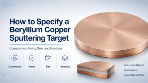
Sputtering plays a critical role in the metallization, buffer layer creation, and contact formation of GaN devices. In this PVD process, high-energy plasma bombards a sputtering target, ejecting atoms that deposit onto the GaN wafer. To achieve optimal electrical contacts (like Ohmic or Schottky contacts) on GaN, engineers rely on ultra-high-purity metallic sputtering targets such as Titanium (Ti), Aluminum (Al), Nickel (Ni), and Gold (Au).
3.4 Electron Beam (E-Beam) Evaporation
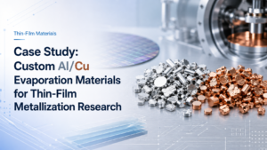
Similar to sputtering, E-Beam Evaporation is a PVD method widely used for contact metallization on GaN wafers. An electron beam melts a crucible of source material, causing it to evaporate and coat the wafer. Using premium evaporation materials guarantees low-resistance contacts, which is crucial for the high-efficiency operation of GaN power devices.
Table 3: Comparison of GaN Thin Film Deposition Techniques
| Deposition Method | Type | Precision Level | Throughput / Scalability | Primary Use Case in GaN Manufacturing |
| MOCVD | Chemical | High | High (Mass Production) | Primary epitaxial growth of GaN and AlGaN layers. |
| MBE | Physical | Atomic (Ultra-High) | Low (R&D / Specialty) | Precise layer control for specialty HEMTs and R&D. |
| Magnetron Sputtering | Physical | Moderate/High | High | Buffer layer deposition; thick metal contact formation. |
| E-Beam Evaporation | Physical | Moderate/High | Moderate/High | High-purity Ohmic and Schottky contact metallization. |
4. Revolutionary Applications of GaN Wafers
The unique properties of GaN translate into massive system-level benefits: smaller form factors, reduced cooling requirements, and higher overall energy efficiency.
4.1 Power Electronics
In the realm of power conversion, GaN is replacing silicon MOSFETs. Because GaN switches can operate at much higher frequencies, the passive components (like capacitors and inductors) required in the circuit can be significantly smaller. This has led to the miniaturization of consumer laptop chargers, high-density server power supplies for data centers, and highly efficient onboard chargers for Electric Vehicles (EVs).
4.2 RF and Microwave Communications
The telecommunications industry relies heavily on GaN-on-SiC wafers. The rollout of 5G networks requires base stations to process more data at higher frequencies. GaN RF power amplifiers provide higher power density, broader bandwidth, and superior thermal performance compared to traditional Silicon LDMOS technology, ensuring reliable cellular coverage.
4.3 Optoelectronics
GaN is the foundational material for the modern lighting industry. Its direct bandgap makes it highly efficient at emitting light in the blue and ultraviolet (UV) spectrums. When combined with phosphors, blue GaN LEDs create the bright white light used in commercial lighting, automotive headlamps, and backlit displays. Furthermore, GaN is critical for producing UV lasers used in data storage and medical sterilization.
5. The TFM Advantage: Your Partner in Thin Film and Semiconductor Materials
Producing high-yield, high-performance GaN devices is incredibly demanding. Even microscopic impurities in the thin film layers or target materials can cause catastrophic device failure. That is why industry leaders partner with Thin Film Materials (TFM).
5.1 Uncompromising Purity and Quality Control
At TFM, we understand that thin film deposition is only as good as the source material. Our high-purity sputtering targets and evaporation materials are refined to strict tolerances (up to 99.999% purity). This ensures minimal outgassing, ultra-low defect densities, and uniform film thickness across your entire GaN wafer batch.
5.2 Customization for Advanced R&D
We do not just offer off-the-shelf products. TFM specializes in custom alloy formulation and precisely machined target geometries to fit specific OEM sputtering systems. Whether you are developing complex AlGaN heterostructures or refining your Ohmic contacts, we can engineer the exact thin film coating materials your process requires.
5.3 Supply Chain Reliability
In a volatile global semiconductor market, consistency is key. TFM offers robust manufacturing capabilities that scale seamlessly from your initial laboratory R&D to full-scale, high-volume commercial production, ensuring you never face material bottlenecks.
6. Conclusion
Gallium Nitride (GaN) wafers are not just a step forward; they are a paradigm shift in how we handle power, light, and data. By overcoming the physical limitations of silicon, GaN-based technologies are making our devices faster, greener, and more efficient. However, mastering GaN manufacturing requires absolute precision in epitaxial growth and thin film deposition.
To achieve the best results, you need the best raw materials. From high-purity metal targets for PVD metallization to advanced materials supporting CVD processes, TFM is dedicated to driving your innovation forward.
Ready to elevate your semiconductor manufacturing process? Contact our engineering team today to Request a Quote and discuss how TFM’s premium sputtering targets and evaporation materials can optimize your GaN device yields.
7. Frequently Asked Questions (FAQs)
Q1: What makes a GaN wafer better than a standard Silicon wafer?
A: GaN has a wider bandgap (3.4 eV vs 1.1 eV for Si), higher electron mobility, and a stronger breakdown field. This allows GaN devices to operate at higher voltages, higher temperatures, and faster switching frequencies with less energy loss than Silicon.
Q2: Why is GaN usually grown on a different substrate like Silicon or SiC?
A: Bulk, free-standing GaN crystals are extremely difficult and expensive to manufacture due to the intense heat and pressure required. Growing a thin layer of GaN on more established, cost-effective substrates (heteroepitaxy) is the most commercially viable method for mass production.
Q3: What is a GaN HEMT?
A: HEMT stands for High Electron Mobility Transistor. It is a specific type of field-effect transistor made using GaN (often an AlGaN/GaN heterojunction) that creates a Two-Dimensional Electron Gas (2DEG). This allows electrons to flow with virtually zero resistance, making HEMTs ideal for high-frequency RF and power applications.
Q4: Which PVD materials are commonly used for GaN metallization?
A: To create electrical contacts on GaN wafers, manufacturers utilize high-purity sputtering targets and evaporation materials. Titanium (Ti), Aluminum (Al), Nickel (Ni), and Gold (Au) are the industry standards for forming Ohmic and Schottky contacts.
Q5: Can TFM provide custom sputtering targets for specific GaN R&D?
A: Yes. TFM specializes in creating custom-formulated alloys and specific geometries tailored to your exact vacuum chamber and deposition requirements. You can browse our semiconductor materials catalog for more information.
Q6: What is the difference between GaN and SiC?
A: Both are wide-bandgap semiconductors, but they excel in different areas. SiC is currently preferred for ultra-high voltage, heavy-duty applications (like EV traction inverters above 800V) due to its incredible thermal conductivity. GaN is unmatched in high-frequency switching and power density for sub-1000V applications (like chargers and RF telecoms).
Q7: How does defect density affect a GaN wafer?
A: Because GaN is often grown on non-native substrates, mismatched crystal lattices cause “threading dislocations” or defects. High defect density can cause current leakage, reduce device efficiency, and shorten the lifespan of the semiconductor. High-quality buffer layers are critical to minimizing these defects.
Q8: What is MOCVD and why is it important for GaN?
A: Metal-Organic Chemical Vapor Deposition (MOCVD) is the primary method used to grow the epitaxial layers of GaN onto a substrate. It allows for the precise, uniform, and scalable deposition of crystalline thin films required for mass-producing LEDs and power transistors.
Q9: Why are GaN wafers primarily used in 5G base stations?
A: 5G requires transmitting massive amounts of data over high-frequency bands (sub-6 GHz and mmWave). GaN-on-SiC RF amplifiers can handle the high power output required for these transmissions while maintaining excellent signal integrity and managing the intense heat generated in the base station.
Q10: Does TFM supply materials for both PVD and CVD processes?
A: Absolutely. TFM provides a comprehensive portfolio of thin film deposition materials, including premium sputtering targets for PVD metallization and specialized source materials to support your advanced CVD and evaporation workflows.