Introduction
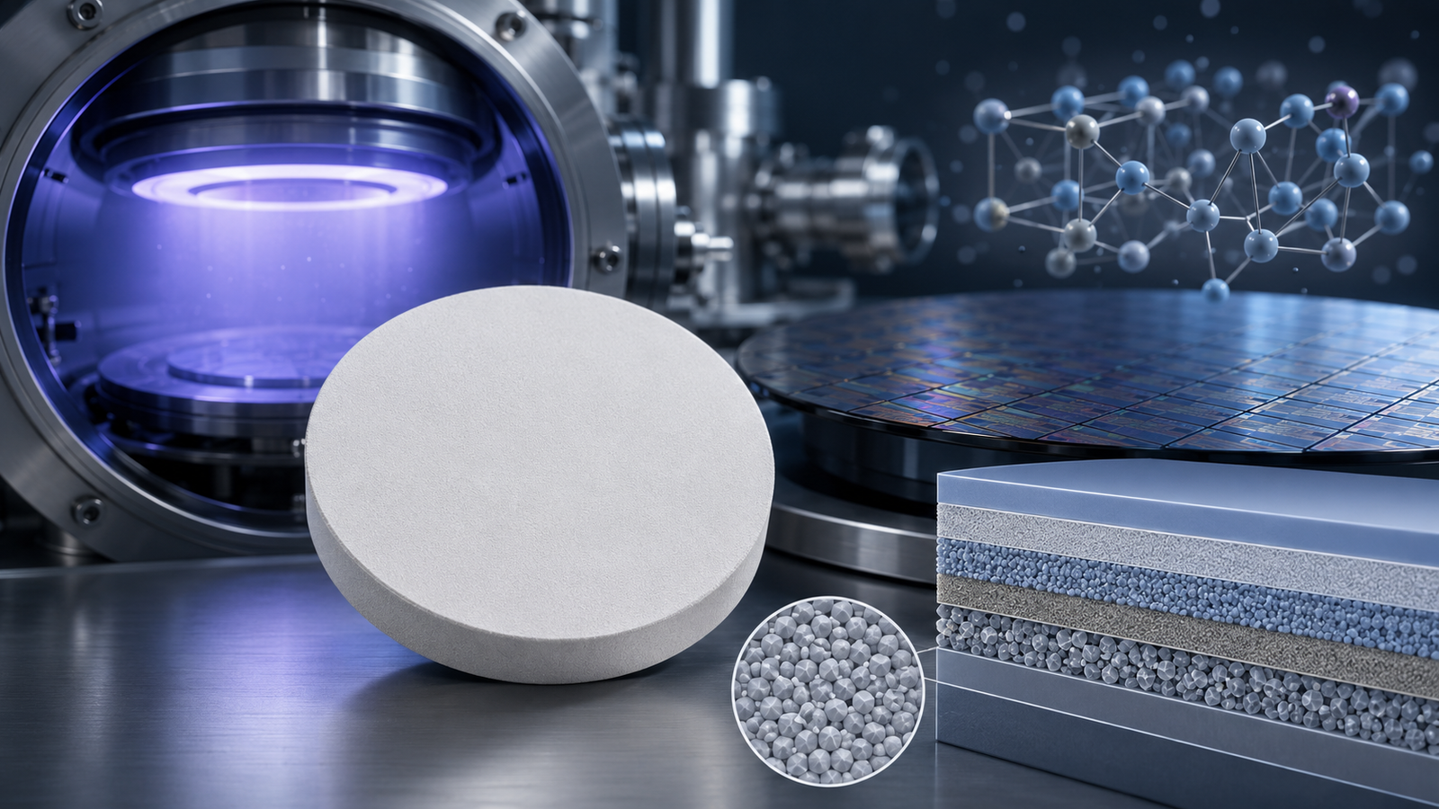
Tungsten sputtering targets are integral to the physical vapor deposition (PVD) processes used in numerous industries. Renowned for their exceptional thermal stability, high melting point, and durability, tungsten sputtering targets enable the creation of thin films on various substrates. These films are critical in applications ranging from semiconductor manufacturing and photovoltaic cells to medical devices and wear-resistant coatings.
This article delves into the unique properties of tungsten sputtering targets, their applications, and the innovations shaping their use in modern technology.
Key Characteristics of Tungsten Sputtering Targets
High Melting Point
Tungsten boasts the highest melting point among all pure metals, at an impressive 3422°C (6192°F). This property makes it an ideal material for sputtering processes that require high temperatures, ensuring structural integrity and consistent performance.
Thermal Stability and Low Vapor Pressure
Tungsten sputtering targets exhibit exceptional thermal stability, maintaining their structure under extreme heat. Their low vapor pressure at elevated temperatures minimizes material loss, resulting in consistent thin film deposition.
Durability and Corrosion Resistance
The high density and hardness of tungsten make it highly durable and resistant to wear. Additionally, its chemical stability ensures corrosion resistance, even in harsh environments, enhancing the longevity of coatings in various applications.
Tungsten Sputtering Target Specifications
| Specification | Details |
| Material Type | Tungsten |
| Symbol | W |
| Color/Appearance | Grayish White, Lustrous, Metallic |
| Melting Point | 3422°C |
| Density | 19.3 g/cm³ |
| Sputter Type | DC |
| Bond Type | Indium, Elastomer |
| Comments | Forms volatile oxides; films are hard and adherent |
| Available Sizes | Diameter: 1.0″–6.0″; Thickness: 0.125″–0.250″ |
Deposition Methods for Tungsten Thin Films
Tungsten (W) thin films are typically deposited using physical vapor deposition (PVD) methods, including sputtering, electron beam evaporation, and pulsed laser deposition. These processes involve the deposition of tungsten atoms onto a substrate to form a thin, uniform layer. Tungsten thin films can also be deposited through chemical vapor deposition (CVD) or atomic layer deposition (ALD), which offer additional techniques for achieving high-quality coatings.
Substrates for Epitaxial Growth of Tungsten Thin Films
Tungsten (W) thin films can be epitaxially grown on a range of substrates, such as single-crystal silicon, gallium arsenide, and aluminum nitride. Silicon is the preferred substrate due to its affordability and accessibility. While less common and more costly, substrates like gallium arsenide and aluminum nitride are also suitable for epitaxial growth of tungsten films.
Substrates for Polycrystalline Tungsten Thin Films
Polycrystalline tungsten thin films can be successfully grown on diverse substrates, including silicon, quartz, glass, and sapphire. These materials provide the necessary foundation for the growth of high-quality polycrystalline films, supporting a variety of industrial and research applications.
Comparison with Other Sputtering Materials
When compared to alternative sputtering materials like molybdenum, aluminum, and copper, tungsten stands out in several ways:
·Molybdenum: Although molybdenum also has excellent high-temperature properties, tungsten surpasses it in durability and melting point, making it better suited for extreme conditions.
·Aluminum: Aluminum offers superior electrical and thermal conductivity for lower-temperature applications. However, tungsten’s robustness ensures longer-lasting performance in high-power scenarios.
·Copper: Copper is favored for its electrical and thermal conductivity, but tungsten’s resistance to thermal stress and slower erosion rate make it ideal for wear-resistant coatings.
Applications of Tungsten Sputtering Targets
Semiconductor Manufacturing
In the semiconductor industry, tungsten sputtering targets are used to deposit thin films for integrated circuits. Their excellent electrical conductivity and resistance to electromigration make tungsten essential for creating conductive barrier layers and interconnects.
Photovoltaic Cells

Tungsten targets play a crucial role in the manufacturing of photovoltaic cells, where they form protective and conductive thin films. These films enhance the efficiency and longevity of solar panels by protecting sensitive materials from environmental damage.
Thin Film Coatings
Tungsten sputtering targets are extensively used for thin film coatings in diverse applications:
·Wear-resistant coatings: Tools and machine components benefit from tungsten films that enhance durability and lifespan.
·Corrosion-resistant coatings: Tungsten coatings protect materials exposed to harsh environments, reducing degradation.
·Decorative coatings: Tungsten films are also used for ornamental finishes, providing a sleek, durable surface.
Medical Devices
In the medical field, tungsten coatings are valued for their radiopacity, which enhances the visibility of implants and tools under X-ray imaging. This property improves the precision of medical procedures and the durability of devices.
Challenges and Innovations
Challenges in Tungsten Sputtering
Despite its advantages, tungsten sputtering faces challenges such as:
·High Melting Point: Operating at elevated temperatures demands advanced equipment and higher energy consumption.
·Film Stress: Tungsten films can develop intrinsic stresses that may lead to cracking or peeling, especially in thick layers.
·Target Bonding Issues: The hardness and brittleness of tungsten complicate its bonding to backing plates, which is critical for effective heat dissipation.
Innovations in Tungsten Sputtering
To address these challenges, several advancements have emerged:
·Advanced Target Bonding Techniques: Methods like diffusion bonding and improved adhesives have enhanced the stability and lifespan of tungsten targets.
·Stress Management Coatings: Using buffer layers and optimizing deposition parameters reduce film stress and improve durability.
·Enhanced Cooling Systems: Modern sputtering systems incorporate advanced cooling mechanisms to handle the high temperatures required for tungsten deposition.
Conclusion
Tungsten sputtering targets are pivotal in advancing modern technology. Their exceptional properties, including high melting point, thermal stability, and durability, make them indispensable in industries such as semiconductors, photovoltaics, and medical devices.
As challenges in tungsten sputtering are addressed through innovations like advanced bonding techniques and stress management coatings, the potential applications for tungsten targets continue to expand. These advancements not only enhance existing technologies but also pave the way for innovative solutions across industries.
For businesses seeking high-quality tungsten sputtering targets, companies like TFM provide expert guidance and cutting-edge products to meet the evolving needs of the market. By leveraging tungsten’s unique properties, industries can achieve superior performance and durability in their products, reinforcing tungsten’s role as a cornerstone of materials science.