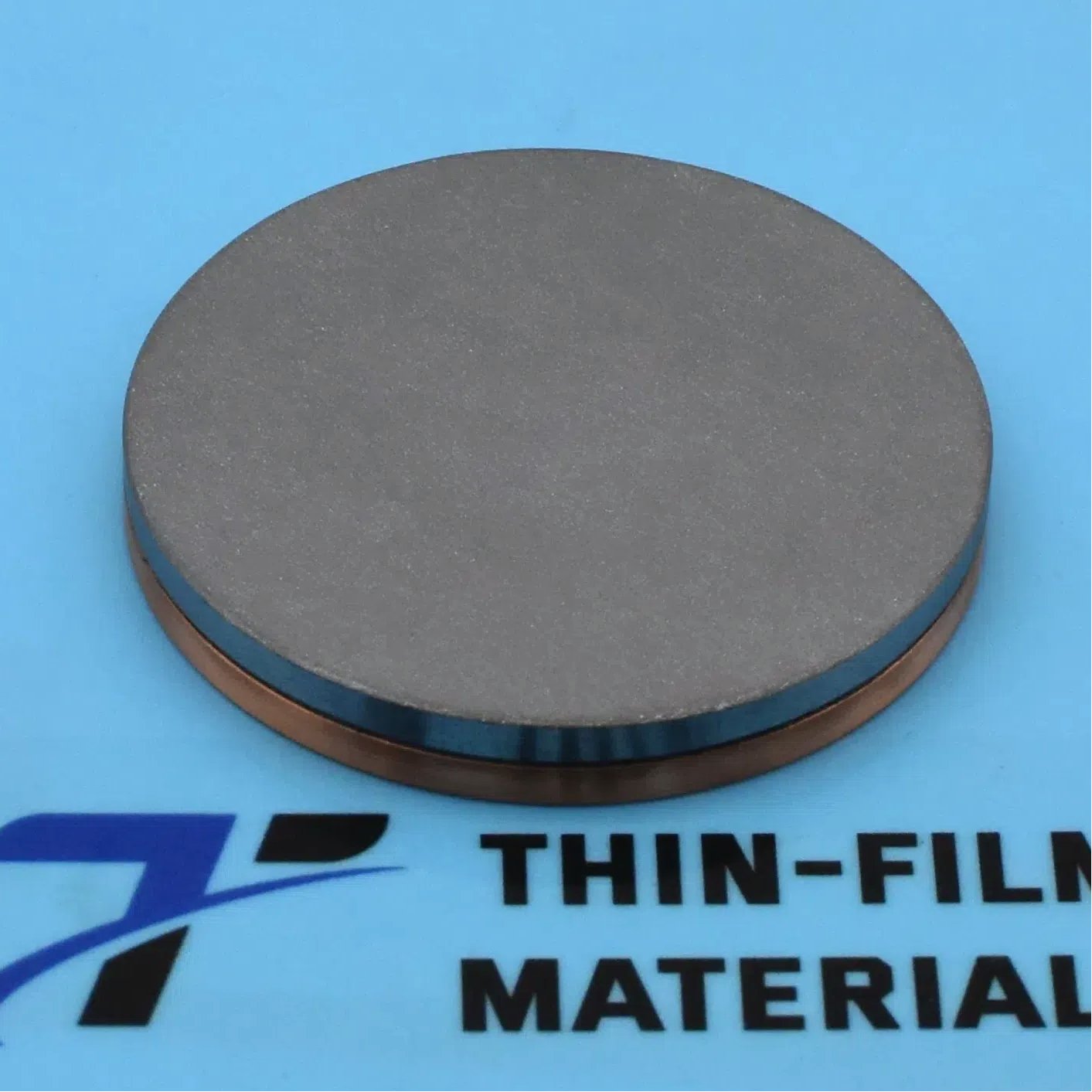

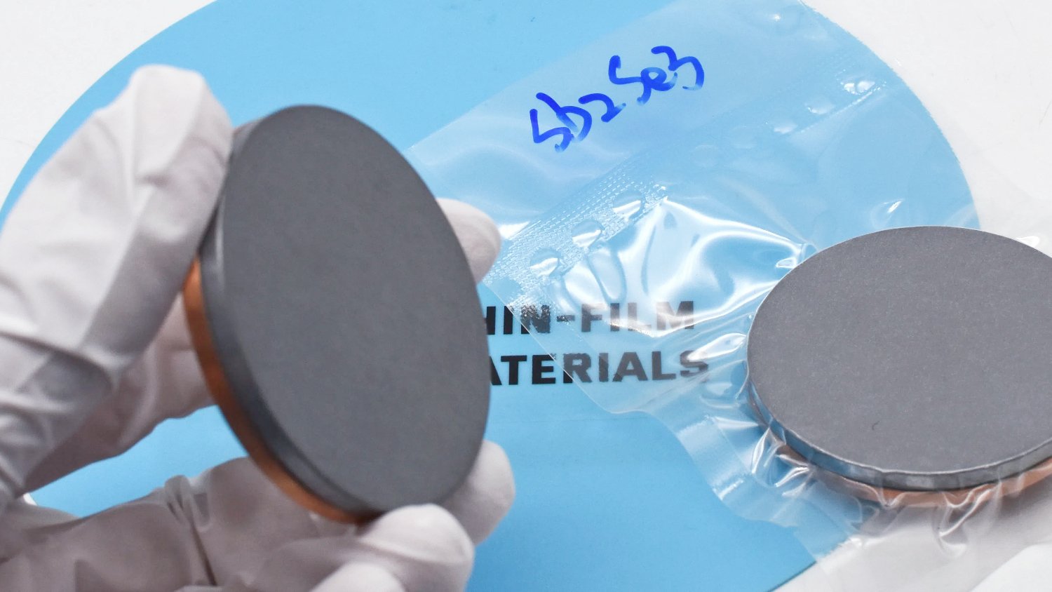
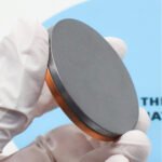
Antimony Triselenide Sputtering Target Description
The Antimony Triselenide Sputtering Target, produced by TFM, is designed with optimal density and a minimal average grain size, making it ideal for use in optoelectronic and thermoelectric technologies. The sputtering process enables the precise deposition of ultra-high purity thin films of metal or oxide materials onto solid substrates. Our targets offer exceptional purity, ensuring the superior quality and performance of the resulting films.
Antimony triselenide, a binary single-phase compound, is particularly well-suited for creating low-cost, low-toxicity solar cells, thanks to its suitable energy bandgap, large absorption coefficient, and low crystal growth temperature. Additionally, its high Seebeck coefficient makes antimony triselenide a promising material for thermoelectric applications, further highlighting its versatility and value in advanced technologies.
Related Product: Antimony Sulfide Sputtering Target, Antimony Telluride Sputtering Target
Antimony Triselenide Sputtering Target Specifications
| Compound Formula | Sb2Se3 |
| Molecular Weight | 480.40 |
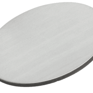
| Appearance | gray target |
| Melting Point | 611℃ |
| Density | 5.81 g/cm3 |
| Available Sizes | Dia.: 1.0″, 2.0″, 3.0″, 4.0″, 5.0″, 6.0″ Thick: 0.125″, 0.250″ |
Antimony Triselenide Sputtering Target Handling Notes
Indium bonding is recommended for the Antimony Triselenide Sputtering Target because of the material’s brittleness and low thermal conductivity, which make it challenging to sputter. These characteristics also make the material prone to thermal shock. Indium bonding helps address these issues, providing enhanced stability and performance during the sputtering process.

Antimony Triselenide Sputtering Target Application
Antimony Triselenide Sputtering Targets are widely used in Chemical Vapor Deposition (CVD), Physical Vapor Deposition (PVD), and various optical processes. Beyond these applications, antimony selenide is also recognized for its potential as a thermoelectric material, thanks to its high Seebeck coefficient. However, its overall efficiency is somewhat limited by its low electrical conductivity, which affects its figure of merit in thermoelectric applications.
Antimony Triselenide Sputtering Target Packaging
Our Antimony Triselenide Sputtering Target is meticulously handled during storage and transportation to ensure it remains in pristine condition. We take every precaution to preserve the quality of our products, so they arrive ready for optimal performance in your applications.

Reviews
There are no reviews yet.