Barium Oxide Sputtering Target (BaO)
Introduction
Barium Oxide (BaO) Sputtering Targets are key materials in thin film deposition, widely applied in advanced electronics, optics, and energy devices. Their high purity and stable physical properties enable uniform thin films with excellent dielectric behavior, making them an essential choice for semiconductor manufacturing and research laboratories.
Detailed Description
Our Barium Oxide Sputtering Targets are manufactured from refined BaO powders using advanced pressing and sintering techniques. This process ensures high density, stable structure, and consistent sputtering results.
Purity: 99.9% (3N) standard, with higher grades available on request
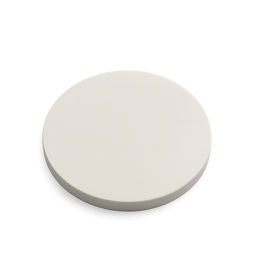
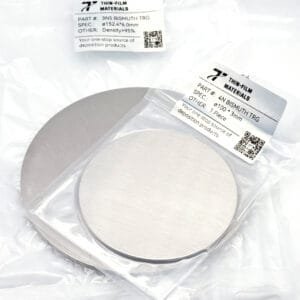
Shapes: Circular, rectangular, and custom-designed targets
Bonding Options: Indium, elastomer, or copper backing plates for enhanced thermal conductivity and target stability
With a melting point of 1,923 °C and a theoretical density of 5.72 g/cc, BaO targets deliver reliable deposition under both RF and DC sputtering systems.
Applications
Barium Oxide Sputtering Targets are used in:
CMOS and semiconductor devices
Gate dielectric and insulating layers
Ferroelectric thin films for memory and capacitors
Optical coatings for displays, sensors, and glass products
Academic and industrial R&D projects
Technical Parameters
| Parameter | Typical Value / Range | Importance |
|---|---|---|
| Purity | 99.9% (3N) | Ensures clean film growth with minimal impurities |
| Diameter | 25 – 300 mm (customizable) | Fits different sputtering system holders |
| Thickness | 3 – 6 mm | Affects sputtering efficiency and deposition rate |
| Bonding | Indium, Elastomer, Copper | Enhances heat transfer and stability |
| Density | 5.72 g/cc (theoretical) | Provides stable sputtering performance |
| Melting Point | 1,923 °C | Suitable for high-temperature processes |
Comparison with Related Materials
| Material | Key Advantage | Typical Application |
|---|---|---|
| Barium Oxide (BaO) | High dielectric constant | Semiconductors, optical coatings |
| Strontium Oxide (SrO) | Good stability, lower reactivity | Dielectric layers |
| Calcium Oxide (CaO) | Cost-effective, easy to handle | General thin film research |
Frequently Asked Questions (FAQ)
| Question | Answer |
|---|---|
| Can I order customized targets? | Yes, dimensions, purity, and bonding options can be tailored. |
| What is the delivery time? | Standard lead time is 2–3 weeks depending on size and quantity. |
| How are the targets packaged? | Vacuum-sealed, with protective foam in export-safe cartons or wooden crates. |
| Which industries use BaO targets? | Mainly semiconductor, optics, energy, aerospace, and university labs. |
Conclusion
Barium Oxide Sputtering Targets provide reliable thin film performance with high dielectric strength and stable deposition. With strict quality control and customizable options, they meet the demands of both research institutions and industrial users.
For detailed specifications and a quotation, please contact us at sales@thinfilmmaterials.com.


Reviews
There are no reviews yet.