Generic selectors
Exact matches only
Search in title
Search in content
Post Type Selectors

VD0671 Barium Titanate Evaporation Materials, BaTiO3

Catalog No.VD0671
MaterialBarium Titanate (BaTiO3)
Purity99.9% ~ 99.99%
ShapePowder/ Granule/ Custom-made

Thin-Film Mat Engineering (TFM) excels in producing and supplying high-purity barium titanate evaporation materials, alongside a broad range of other evaporation materials. Our offerings include both powder and granule forms, with custom solutions available to meet specific requirements upon request.

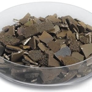
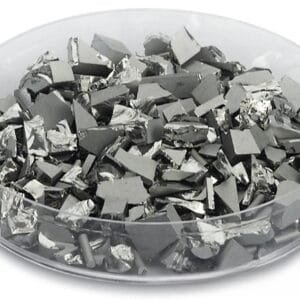
Barium Titanate Evaporation Materials Overview

Thin-Film Mat Engineering (TFM) offers high-purity barium titanate evaporation materials with the chemical formula BaTiO3. These materials are vital for achieving high-quality films in deposition processes. TFM specializes in producing evaporation materials with purity levels up to 99.9995%, ensuring exceptional reliability through stringent quality assurance measures.

Related Products: Barium Evaporation Materials, Titanium Evaporation Materials

Barium Titanate Evaporation Materials Specifications

Crystal structure

Tetragonal

Density

6.02g/cm3

Melting Point

1600 °C

Molecule mass (g/mol)

233.192

Dielectric constants:

ea = 3700, ec = 135 (unclamped)

ea = 2400, ec = 60 (clamped)

Index of Refraction

515nm 633nm 800nm
No 2.4912 2.4160 2.3681
Ne 2.4247 2.3630 2.3235

Reflectivity of SPPC ( at 0 deg. cut )

50-70% (max. 77%) for l = 515 nm

50-80% (max: 86.8%) for l = 633 nm

Thermal Expansion

9.4 x 10⁻⁶ /℃

Crystal orientation

<100>、<110>、<111>

Standard Size

 5x5mm, 10x10mm, Or customized.

Standard Thickness

0.5mm, 1.0mm,

Polishing

Single side polished or Double side polished

Applications

Barium titanate evaporation materials are extensively used in:

  • Deposition Processes: Essential for semiconductor deposition, chemical vapor deposition (CVD), and physical vapor deposition (PVD).
  • Optics: Applied in wear protection, decorative coatings, and display technologies.

Packaging and Handling

Our barium titanate evaporation materials are meticulously tagged and labeled to ensure proper identification and maintain high standards of quality control. We take great care to prevent any damage during storage and transportation.

Contact Us

Thin-Film Mat Engineering (TFM) is a leading supplier of high-purity barium titanate evaporation materials. We offer various forms, including tablets, granules, rods, and wires, with custom shapes and quantities available upon request. We also provide evaporation sources, boats, filaments, crucibles, heaters, and e-beam crucible liners. For current pricing and inquiries about materials not listed, please contact us directly.

Reviews

There are no reviews yet.

Be the first to review “VD0671 Barium Titanate Evaporation Materials, BaTiO3”

Your email address will not be published. Required fields are marked *

FAQ

  • They are high‐purity substances (e.g. metals, alloys, or compounds) used in thermal or electron‐beam evaporation processes to form thin films on substrates.

  • Typically, they’re processed into a form (often ingots, pellets, or wires) that can be efficiently vaporized. Preparation emphasizes high purity and controlled composition to ensure film quality.

  • Thermal evaporation and electron-beam (e-beam) evaporation are the two main techniques, where material is heated (or bombarded with electrons) until it vaporizes and then condenses on the substrate.

  • Thermal evaporation heats the material directly (often using a resistive heater), while e-beam evaporation uses a focused electron beam to locally heat and vaporize the source material—each method offering different control and energy efficiency.

  • Key parameters include source temperature, vacuum level, deposition rate, substrate temperature, and the distance between the source and the substrate. These factors influence film uniformity, adhesion, and microstructure.

  • Evaporation generally produces high-purity films with excellent control over thickness, and it is especially suitable for materials with relatively low melting points or high vapor pressures.

  • Challenges include issues with step coverage (due to line-of-sight deposition), shadowing effects on complex topographies, and possible re-evaporation of material from the substrate if temperature isn’t properly controlled.

  • Common evaporation materials include noble metals (e.g., gold, silver), semiconductors (e.g., silicon, germanium), metal oxides, and organic compounds—each chosen for its specific optical, electrical, or mechanical properties.

  • Selection depends on desired film properties (conductivity, optical transparency, adhesion), compatibility with the evaporation process, and the final device application (semiconductor, optical coating, etc.).

  • Optimizing substrate temperature, deposition rate, and chamber vacuum are critical for ensuring that the film adheres well and forms the intended microstructure without defects.

  • Troubleshooting may involve checking the source material’s purity, ensuring stable source temperature, verifying the vacuum level, adjusting the substrate’s position or temperature, and monitoring deposition rate fluctuations.

While evaporation tends to yield very high purity films with excellent thickness control, it is limited by its line-of-sight nature. In contrast, sputtering can deposit films more uniformly on complex surfaces and is more versatile for a broader range of materials.


Shopping Cart
Scroll to Top