 MSDS File
| Material Type | Beryllium |
| Symbol | Be |
| Atomic Weight | 9.0121831 |
| Atomic Number | 4 |
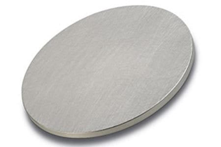
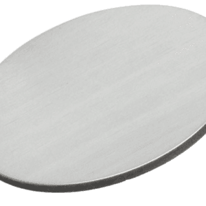
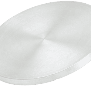
| Color/Appearance | White-gray Metallic |
| Thermal Conductivity | 201 W/m.K |
| Melting Point (°C) | 1278 |
| Coefficient of Thermal Expansion | 11.3 x 10⁻⁶/K |
| Theoretical Density (g/cc) | 1.85 |
| Z Ratio | |
| Sputter | RF, DC |
| UN Number | 1567 |
Overview of Beryllium Sputtering Targets
Introduction to Beryllium Sputtering Targets
Beryllium, symbolized as Be, is a rare chemical element with atomic number 4. As an alkaline earth metal, it is typically found in minerals in combination with other elements. Beryllium is used in various applications, including as an inherent filter in X-ray tubes to determine X-ray energy. Beryllium is a steel-gray, lightweight, and brittle material that is often used for its unique properties in electronics, semiconductors, and flat-panel displays.
Key Properties of Beryllium Sputtering Targets
- Material Type: Beryllium
- Symbol: Be
- Atomic Weight: 9.0122
- Atomic Number: 4
- Appearance: Steel-gray, strong, and brittle
- Purity: 98.5% – 99.9%
- Thermal Conductivity: 200 W/m.K
- Density: 1.848 g/cc
- Sputtering Method: PDC
- Max Power Density: 80 W/in²
- Bonding Options: Indium, Elastomer
Manufacturing Process
- Refining: Three-layer electrolytic process to ensure high purity.
- Melting and Casting: Semi-continuous casting using an electrical resistance furnace.
- Grain Refinement: Achieved through thermomechanical treatment for engineered microstructures.
- Final Packaging: Cleaned for vacuum use and protected from contaminants during shipping.
Product Specifications
- Purity: 98.5% – 99.9%
- Circular Dimensions: Up to 14-inch diameter, minimum 1 mm thickness.
- Block Dimensions: Up to 32-inch length, 12-inch width, minimum 1 mm thickness.
Features and Benefits
- High Purity: Ensures exceptional performance for high-precision applications.
- Refined Grain Structure: Offers improved sputtering characteristics.
- Competitive Pricing: Cost-effective for a variety of industries.
- Semiconductor Grade: Suitable for semiconductor and advanced electronic applications.
Applications
Beryllium sputtering targets are used in:
- Electronics
- Semiconductor Manufacturing
- Flat Panel Displays
Additional Options
- 98.5% Minimum Purity
- Smaller Sizes: Available for research and development applications.
- Bonding Services: Indium and elastomer bonding for specialized requirements.
Inquiry Form
Required Information
- Name
- Email ID
- Company Name
- Industry
Optional Information
- Phone Number
- Address
- Country
- Details About Material Requirements

Reviews
There are no reviews yet.