
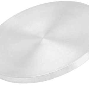
Bismuth Antimony Selenide Sputtering Target Description
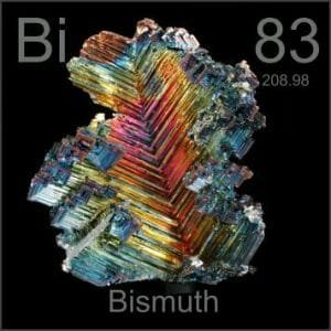
Bismuth is a chemical element named after the German *Bisemutum*, a corruption of *Weisse Masse*, meaning “white mass.” It was first used in 1753 and discovered by C.F. Geoffroy. The chemical symbol for bismuth is “Bi.” It is located in Period 6, Group 15 of the periodic table, within the p-block. Its atomic number is 83, and its relative atomic mass is 208.98040, with the number in brackets indicating the uncertainty.
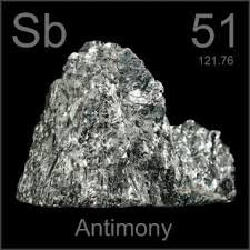
Antimony is a lustrous gray metalloid primarily found as the sulfide mineral stibnite (Sb₂S₃). Antimony compounds have been known since ancient times and were used in medicine and cosmetics, often referred to by the Arabic name *kohl*. Metallic antimony was also recognized early on but was mistakenly identified as lead. The earliest known description of the metal in the West was by Vannoccio Biringuccio in 1540. Industrial refining methods for antimony include roasting and reduction with carbon, or direct reduction of stibnite with iron.
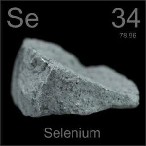 Selenium is a chemical element named after the Greek word *selene*, meaning “moon.” It was first mentioned in 1817 by J. Berzelius and G. Gahn, who also accomplished its isolation. The chemical symbol for selenium is “Se.” It is located in Period 4, Group 16 of the periodic table, within the p-block. Its atomic number is 34, and its relative atomic mass is 78.96, with the number in brackets indicating the uncertainty.
Related Products: Bismuth Sputtering Target, Antimony Sputtering Target
Bismuth Antimony Selenide Sputtering Target Specifications
| Material Type | Bismuth Antimony Selenide |
| Symbol | Bi/Sb/Se |
| Color/Appearance | Solid |
| Melting Point | / |
| Density | / |
| Available Sizes | Dia.: 2.0″, 3.0″, 4.0″, 5.0″, 6.0″ Thick: 0.125″, 0.250″ |
We also offer other customized shapes and sizes of the sputtering targets; please Contact Us for more information.
Packing
Our Bismuth Antimony Selenide Sputtering Targets are clearly tagged and labeled for efficient identification and quality control. We take great care to prevent any damage during storage and transportation, ensuring the targets remain in excellent condition.
Get Contact
TFM offers Bismuth Antimony Selenide Sputtering Targets in various forms, purities, sizes, and prices. We specialize in high-purity thin film deposition materials with optimal density and minimal grain sizes, which are ideal for semiconductor, CVD, and PVD applications in display and optics. Contact Us for current pricing on sputtering targets and other deposition materials that are not listed.


Reviews
There are no reviews yet.