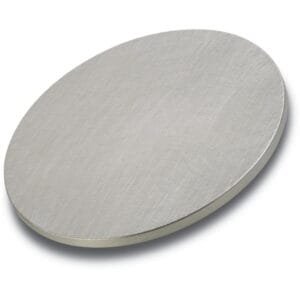
Bismuth Antimony Telluride P-Type Sputtering Target
Introduction
The Bismuth Antimony Telluride P-Type Sputtering Target (Bi₀.₅Sb₁.₅Te₃) is a core material for thermoelectric thin films used in energy harvesting, solid-state cooling, and high-precision thermal management devices. Its P-type characteristics—achieved through controlled Sb doping—enable strong Seebeck performance and excellent compatibility with semiconductor manufacturing processes.
Detailed Description
This sputtering target is produced with a carefully engineered Bi–Sb–Te composition, offering optimized hole concentration and improved thermoelectric power factor.
P-type thermoelectric alloy: The substitution of Bi with Sb enhances hole mobility, providing superior P-leg performance in thin-film thermoelectric devices.
High-density microstructure: Fabricated through vacuum sintering, hot pressing, or HIP to ensure high densification and minimal porosity, essential for stable sputtering erosion.
Consistent sputtering behavior: The balanced stoichiometry minimizes Te loss during deposition, resulting in uniform film thickness and reproducible thermoelectric efficiency.
High purity: Available from 3N (99.9%) to 5N (99.999%) purity, supporting research-grade and production-level requirements.
The result is a target optimized for next-generation thermoelectric films where electrical performance, adhesion quality, and film reliability are essential.
Applications
Thin-film thermoelectric modules (P-leg materials)
Micro-coolers and solid-state cooling devices
Energy harvesting and thermal-electric generators
Infrared sensors and microelectronic thermal control films
MEMS thermoelectric components
Research on Bi–Sb–Te alloy systems
Technical Parameters
| Parameter | Typical Value / Range | Importance |
|---|---|---|
| Purity | 99.9% – 99.999% | Clean films and higher thermoelectric performance |
| Composition | Bi₀.₅Sb₁.₅Te₃ (P-type) | Provides optimized hole concentration |
| Diameter | 25 – 300 mm (custom) | Compatible with a wide range of sputtering systems |
| Thickness | 3 – 6 mm | Affects erosion rate and target lifetime |
| Density | ≥ 95% theoretical | Ensures homogenous sputtering |
| Bonding | Indium / Elastomer / Copper | Improves cooling and prevents cracking |
Comparison with Related Materials
| Material | Key Advantage | Typical Application |
|---|---|---|
| Bi₀.₅Sb₁.₅Te₃ (P-type) | High P-leg performance, stable hole mobility | Thermoelectric devices |
| Bi₂Te₂.₇Se₀.₃ (N-type) | Strong Seebeck coefficient, optimized electron concentration | Complementary N-leg films |
| Bi₂Te₃ | Economical, widely studied | General thermoelectric R&D |
FAQ
| Question | Answer |
|---|---|
| Can you customize the size and purity? | Yes. Diameter, thickness, purity grade, and bonding are fully customizable. |
| What is the standard packaging? | Vacuum-sealed, foam-protected, and shipped in export-safe cartons or wooden crates. |
| Which systems can it be used on? | Suitable for DC/RF magnetron sputtering systems used in thermoelectric and semiconductor research. |
| Does the stoichiometry influence film behavior? | Yes. Bi/Sb/Te ratio directly affects P-type carrier concentration and Seebeck performance. |
| Should large targets be bonded? | Yes, bonding improves heat transfer and prevents warping/cracking during sputtering. |
Packaging
All Bismuth Antimony Telluride P-Type Sputtering Targets are vacuum-sealed and clearly labeled for traceability. Additional cushioning and rigid external packaging prevent chipping, oxidation, or mechanical damage during transport.
Conclusion
The Bi₀.₅Sb₁.₅Te₃ P-Type Sputtering Target provides high thermoelectric efficiency, stable film deposition behavior, and strong compatibility with advanced semiconductor processes. Available in multiple purities and customizable dimensions, it is a reliable solution for both R&D and industrial thin-film production.
For detailed specifications or a quotation, please contact us at sales@keyuematerials.com.


Reviews
There are no reviews yet.