
 MSDS File
Introduction
Copper Aluminum (Cu/Al) evaporation materials are widely used in thin film deposition processes for creating conductive, reflective, and functional alloy coatings. By combining copper’s excellent electrical conductivity with aluminum’s lightweight nature and oxidation resistance, Cu/Al materials offer a balanced solution for advanced coating applications in electronics, optics, and industrial technologies. High-quality evaporation materials are essential to ensure stable evaporation behavior and consistent film composition.
Detailed Description
Copper Aluminum evaporation materials are typically supplied as alloyed mixtures or co-evaporation combinations, depending on the required film composition and process control. The Cu/Al ratio can be precisely tailored to meet specific electrical, thermal, and mechanical performance requirements.
Copper contributes high electrical and thermal conductivity, making it ideal for conductive layers and interconnects. Aluminum, on the other hand, provides excellent oxidation resistance, low density, and good adhesion to various substrates. When combined, Cu/Al thin films can achieve improved corrosion resistance, enhanced mechanical stability, and tunable conductivity.
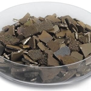
These materials are manufactured through vacuum melting or powder metallurgy processes to ensure compositional uniformity and high purity. Forms such as pellets, granules, wires, or pre-alloyed pieces are available for compatibility with thermal evaporation or electron beam evaporation systems. Controlled particle size and material density help maintain stable evaporation rates and reduce spitting during deposition.
In applications requiring precise composition control, co-evaporation using separate Cu and Al sources can also be implemented, allowing dynamic adjustment of film stoichiometry during deposition.
Applications
Copper Aluminum Evaporation Materials are widely used in:
- Semiconductor Metallization: Interconnects and conductive layers
- Thin Film Electronics: Functional coatings with tailored conductivity
- Optical Coatings: Reflective and protective layers
- Decorative Coatings: Durable and corrosion-resistant finishes
- Energy Devices: Components in batteries and photovoltaic systems
Technical Parameters
| Parameter | Typical Value / Range | Importance |
|---|---|---|
| Composition | Cu/Al (custom ratios) | Determines electrical and mechanical properties |
| Purity | 99.9% – 99.99% (3N – 4N) | Ensures film quality and consistency |
| Form | Pellets / Granules / Wire / Pieces | Compatible with evaporation systems |
| Particle Size | 1 – 6 mm (granules) / custom | Affects evaporation stability |
| Density | High-density or pre-alloyed | Improves evaporation uniformity |
| Evaporation Method | Thermal / E-beam / Co-evaporation | Process flexibility |
Comparison with Related Materials
| Material | Key Advantage | Typical Application |
|---|---|---|
| Cu/Al Alloy | Balanced conductivity and corrosion resistance | Electronics, coatings |
| Copper (Cu) | Excellent conductivity | Interconnects |
| Aluminum (Al) | Lightweight, oxidation resistant | Reflective coatings |
| Cu-Ni Alloy | Enhanced corrosion resistance | Marine and industrial coatings |
FAQ
| Question | Answer |
|---|---|
| Can the Cu/Al ratio be customized? | Yes, the composition can be tailored to meet specific application requirements. |
| Is pre-alloyed material better than co-evaporation? | Pre-alloyed materials provide uniform composition, while co-evaporation offers more flexibility in adjusting ratios. |
| What evaporation methods are supported? | Thermal and electron beam evaporation are both suitable. |
| How is material stability ensured during evaporation? | Controlled purity, particle size, and density help maintain stable evaporation behavior. |
| Which industries use Cu/Al evaporation materials? | Semiconductor, electronics, optics, energy, and decorative coating industries. |
Packaging
Our Copper Aluminum Evaporation Materials, Cu/Al, are meticulously tagged and labeled externally to ensure efficient identification and maintain high standards of quality control. We take great care to prevent any potential damage during storage and transportation, ensuring the materials arrive in optimal condition.
Conclusion
Copper Aluminum Evaporation Materials provide a versatile and reliable solution for producing high-performance thin films with tailored electrical and mechanical properties. With customizable compositions, high purity, and stable evaporation characteristics, Cu/Al materials are ideal for both industrial production and research applications.
For detailed specifications and a quotation, please contact us at sales@thinfilmmaterials.com.


Reviews
There are no reviews yet.