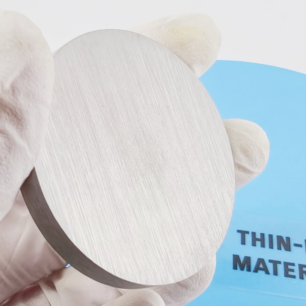
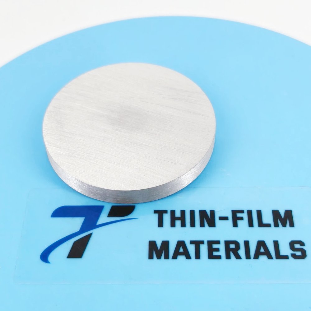
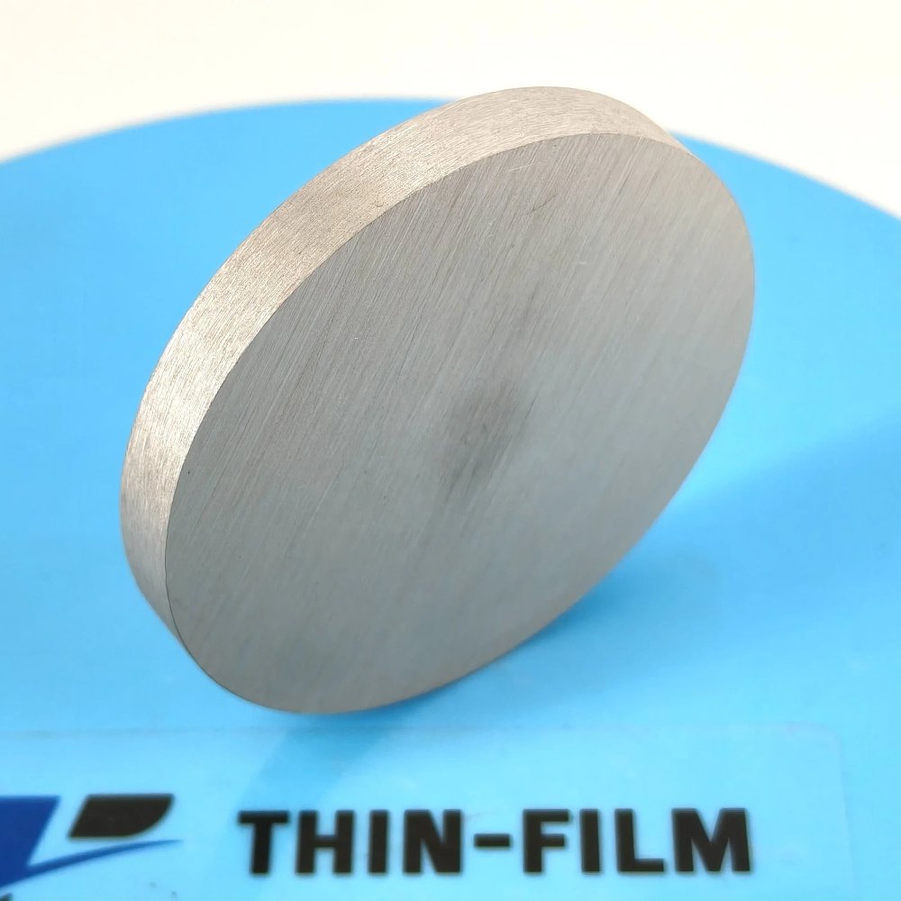

Copper Indium Gallium Sputtering Target Description
The Copper Indium Gallium Sputtering Target is employed in thin film deposition processes, made from a blend of copper (Cu), indium (In), and gallium (Ga). In sputtering, material is ejected from the target surface and deposited onto a substrate to create a thin film.
This target is primarily used in the production of Copper Indium Gallium Selenide (CIGS) solar cells. These thin-film photovoltaic devices are known for their high efficiency and flexibility, making them ideal for applications like building-integrated photovoltaics.
Copper Indium Gallium Sputtering Target Specifications
| Compound Formula | Cu/In/Ga |
| Appearance | Metallic target |
| Molecular Weight | 248.087 |
| Available Sizes | Dia.: 1.0″, 2.0″, 3.0″, 4.0″, 5.0″, 6.0″ Thick: 0.125″, 0.250″ |
Copper Indium Gallium Sputtering Target Handling Notes
Indium bonding is recommended for the Copper Indium Gallium Sputtering Target due to its characteristics that can pose challenges during sputtering, such as brittleness and low thermal conductivity. The material’s low thermal conductivity makes it susceptible to thermal shock, so indium bonding helps improve its performance and stability during the sputtering process.
Copper Indium Gallium Sputtering Target Application
The Copper Indium Gallium Sputtering Target is essential for manufacturing Copper Indium Gallium Selenide (CIGS) solar cells, which are thin-film photovoltaic devices. CIGS solar cells are known for their high efficiency and flexibility, making them ideal for diverse applications, including building-integrated photovoltaics.
Copper Indium Gallium Sputtering Target Packaging
We take great care in handling our Copper Indium Gallium Sputtering Targets during storage and transportation to ensure they maintain their quality and remain in their original condition.


Reviews
There are no reviews yet.