

Gallium Oxide (Ga₂O₃) Sputtering Target
High-Purity Ceramic Targets for UV Detection, Oxide Semiconductor, Optical, and Sensor Films
High-purity gallium oxide sputtering targets for Ga₂O₃ thin-film research in solar-blind UV detection, oxide semiconductor studies, optical coatings, sensors, and emerging device development. Available in planar, step, bonded, unbonded, and drawing-specific configurations.
- Standard purity option: 99.99% (4N)
- Planar, bonded, and custom assemblies
- RF sputtering commonly used
- CoA and inspection support available

Quick Specifications
| Item | Available / Information to Confirm |
|---|---|
| Material | Gallium(III) Oxide, Ga₂O₃ |
| CAS Number | 12024-21-4 |
| Purity | Standard purity option: 99.99% (4N); other purity or impurity-control requirements subject to review |
| Composition / Doping | Undoped Ga₂O₃ or specified doped / mixed-oxide composition |
| Target Phase | β-Ga₂O₃ or another agreed phase / XRD requirement where specified |
| Forms | Disc, rectangular plate, step target, bonded assembly, and drawing-specific geometry |
| Density / Resistivity | Measured value, minimum requirement, or report scope should be stated separately |
| Bonding | Unbonded or bonded to a reviewed backing-plate design; bond system and operating limits should be confirmed |
| Sputtering Mode | RF magnetron sputtering is commonly used; DC or pulsed-DC compatibility depends on conductivity, dopant level, equipment, and process conditions |
| Documentation | CoA, dimensional inspection, density, XRD / phase, resistivity, and bonding records where agreed |
Have a standard size, bonded assembly, or custom cathode requirement?
Product Overview
A gallium oxide sputtering target is used as a source material for depositing Ga₂O₃-based thin films in UV detection, oxide semiconductor research, optical coatings, sensors, and related functional oxide studies. For ordering, the target should be specified by composition, purity, phase or XRD requirement, density, dimensions, bonding design, and documentation scope.
Ga₂O₃ is widely studied as an ultra-wide-bandgap oxide semiconductor, especially for solar-blind UV detection and emerging electronic-device research. For sputtered films, the final structure and properties also depend on substrate, oxygen condition, sputtering power, temperature, thickness, and annealing.
View the wider Ceramic Sputtering Targets range.
Technical Note: Target Specification vs Film Result
Ga₂O₃ target composition, purity, phase, density, resistivity, bonding, and cathode fit are important order-acceptance criteria. However, deposited-film phase, crystallinity, stoichiometry, roughness, bandgap, and electrical properties also depend on the sputtering process, substrate, gas atmosphere, temperature, film thickness, and annealing route.
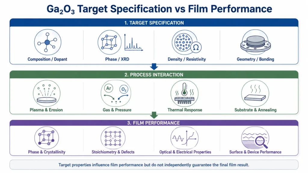
Available Gallium Oxide Target Configurations
The four formats below cover most laboratory, replacement, production, and custom Ga₂O₃ sputtering inquiries. Each format should be reviewed against the actual cathode and cooling interface.
Standard Circular Planar Targets
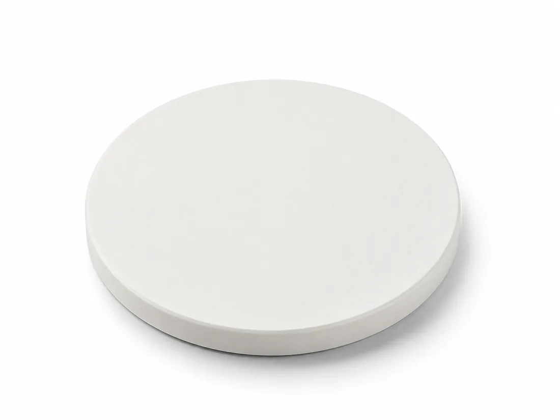
Use: Laboratory RF magnetrons and standard planar cathodes.
Confirm: Diameter, ceramic thickness, purity, density, edge condition, mounting, and tolerance.
Rectangular & Step Targets
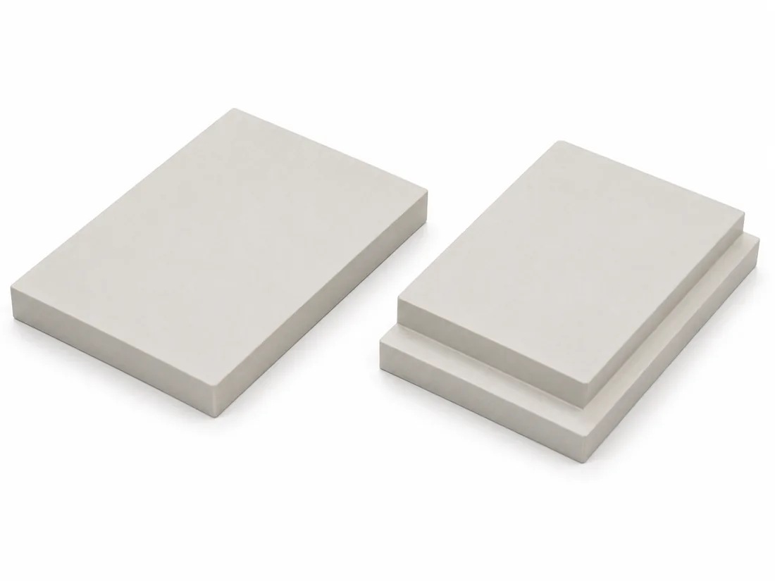
Use: Inline coaters, custom magnetrons, and replacement projects.
Confirm: L × W, thickness, step, shoulder, edge profile, flatness, and erosion zone.
Bonded Target Assemblies
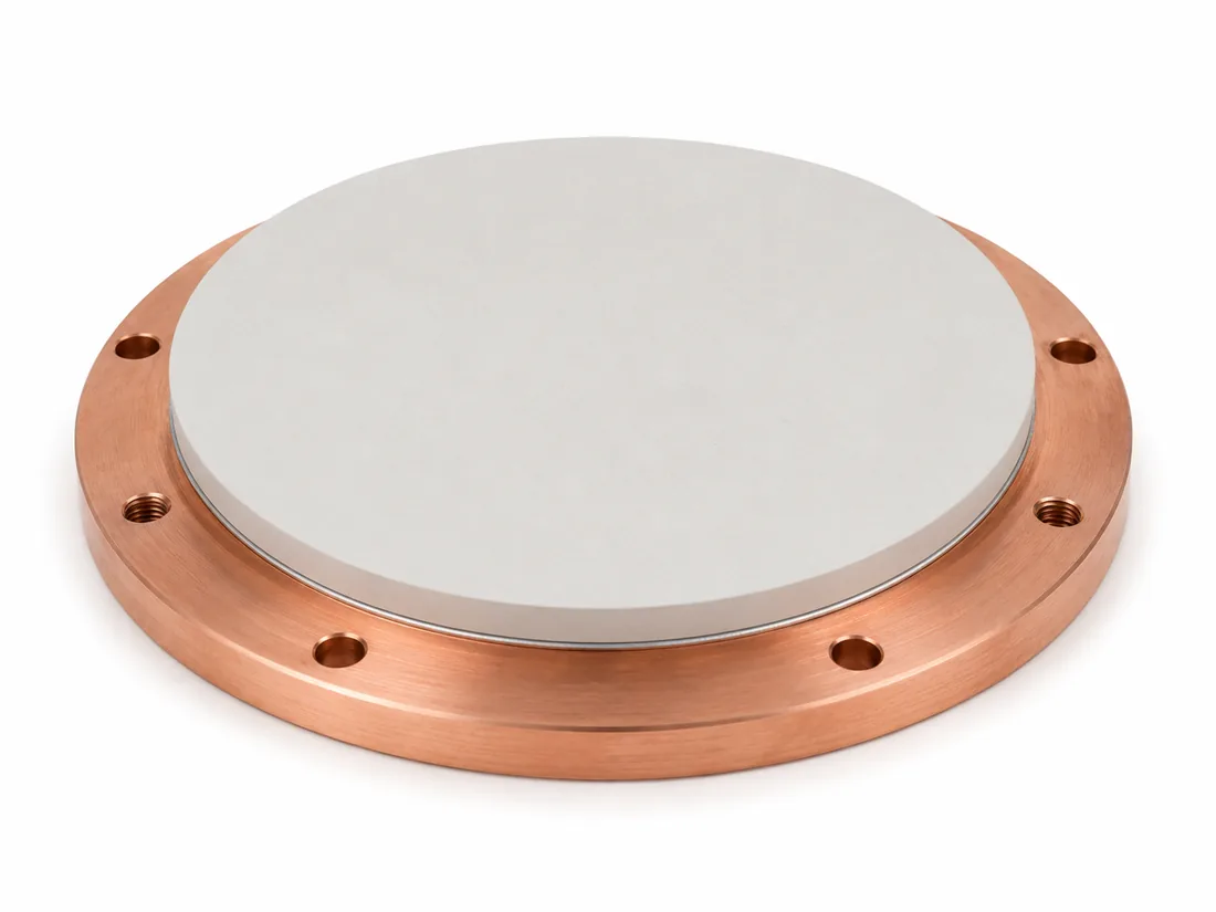
Use: Projects requiring added mechanical support or a controlled thermal interface.
Confirm: Ceramic thickness, bond material, backing dimensions, holes, PCD, total thickness, intended power, and cooling condition.
Drawing-Specific Replacement Targets
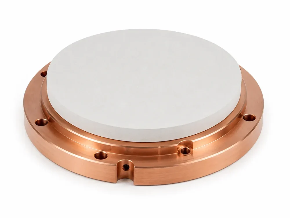
Use: Existing cathodes or assemblies that must be reproduced to fit.
Confirm: Source manufacturer, model, installed height, cooling interface, current target photo, and acceptance drawing.
Additional custom options: Doped Ga₂O₃, mixed-oxide compositions, segmented targets, customer-supplied backing plates, special hole patterns, phase-specific requirements, and customer-format documents may be reviewed according to material and technical feasibility.
For bonded or replacement assemblies, see Sputtering Target Bonding Service or send the target drawing for review.
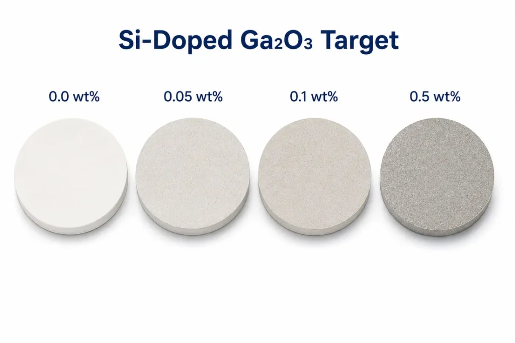
Doped and Mixed-Oxide Options
Doped Ga₂O₃ targets, such as Si-doped Ga₂O₃, may be reviewed when the dopant concentration, calculation basis, target phase, density, size, and documentation requirements are clearly stated.
Composition note: dopant concentration, calculation basis, phase, density, dimensions, and availability must be confirmed for each order.
Gallium Oxide Sputtering Target Applications
Each application should be reviewed by film role, why Ga₂O₃ is selected, and the specifications required before quotation.
Solar-Blind UV Photodetectors
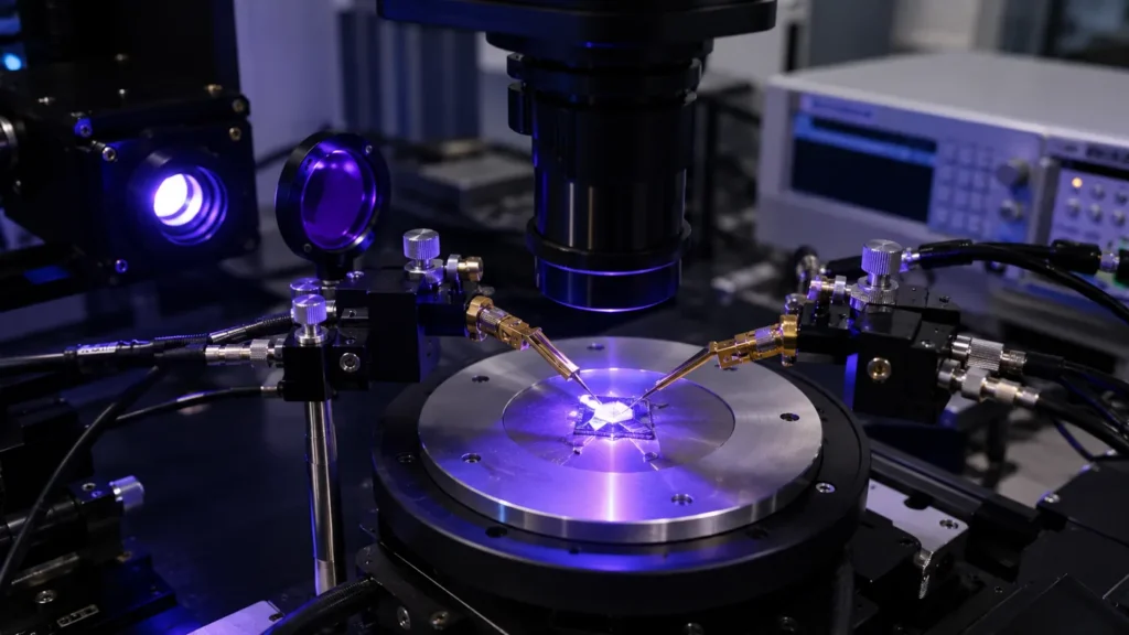
Film role: Active or photoresponsive Ga₂O₃ layer in UV-C / solar-blind detector structures.
Why Ga₂O₃: Its ultra-wide bandgap and low visible-light response make it a research candidate for selective deep-UV detection.
Confirm: Wavelength range, phase, thickness, substrate, oxygen condition, annealing, and electrode design.
Oxide Semiconductor & Emerging Device Research

Film role: Functional oxide layer, buffer layer, interface layer, or exploratory semiconductor film in early-stage device studies.
Why Ga₂O₃: Ga₂O₃ is studied as an ultra-wide-bandgap oxide semiconductor. Sputtered films are often used for exploratory thin-film research, interface studies, and device-development experiments rather than as a universal route for bulk-like high-power Ga₂O₃ devices.
Confirm: Layer function, substrate, crystallinity target, doping, oxygen condition, thermal budget, and post-deposition treatment.
UV Optical & Functional Oxide Films
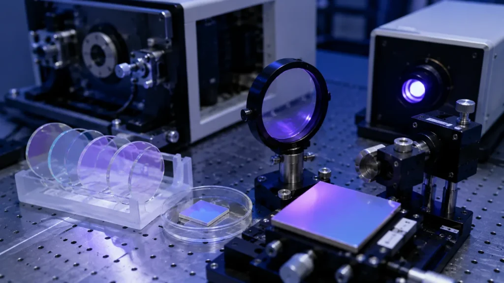
Film role: Transparent current-spreading layer or conductive contact in LEDs, photodetectors, emitters, and optoelectronic devices.
Why Ga₂O₃: Selected where current spreading and optical transmission are required in the same layer and the contact stack has been qualified for Ga₂O₃.
Confirm: Device structure, contact role, required resistance, transmission range, thickness, surface roughness, substrate temperature, and annealing.
Smart Windows & Functional Glass

Film role: Transparent electrode, heater, antistatic layer, or conductive component in electrochromic and optical glass stacks.
Why Ga₂O₃: Suited to transparent conductive functions where sheet resistance, optical neutrality, durability, and large-area uniformity are defined together.
Confirm: Coated area, planar or rotary cathode, sheet resistance, optical range, durability test, glass size, line dimensions, and production rate.
Explore TFM’s Thin-Film Applications for additional device and coating examples.
How to Select a Gallium Oxide Sputtering Target
| Selection Factor | What to Confirm | Why It Matters |
|---|---|---|
| Intended Film | UV detector, oxide semiconductor, optical, sensor, buffer, or functional oxide layer | Defines target route, substrate, process window, and film-evaluation method |
| Composition / Dopant | Undoped Ga₂O₃ or specified doped / mixed oxide with stated calculation basis | Dopants and secondary oxides can alter conductivity, phase behavior, and sintering response |
| Purity & Impurities | 4N purity option or customer-specific impurity limits | Trace elements may affect optical absorption, conductivity, defects, and interfaces |
| Target Phase / XRD | β phase, mixed phase, another phase requirement, or no phase requirement | Useful for incoming inspection, but not a standalone film-phase guarantee |
| Density / Porosity | Measured bulk density, relative density, or minimum accepted value | Porosity may affect strength, particle tendency, erosion, and bonding behavior |
| Resistivity / Power Mode | Measured target resistivity where needed; RF, DC, or pulsed-DC review | Power compatibility depends on actual target, power supply, cathode, and gas process |
| Geometry / Bonding / Cathode | Dimensions, installed height, backing plate, bond, holes, PCD, cooling, and erosion zone | Controls fit, support, thermal contact, and allowable operation |
| Process Route | Ar or Ar/O₂, pressure, substrate, temperature, annealing, and film thickness | Strongly affects stoichiometry, crystallinity, roughness, optical response, and conductivity |
| Acceptance & Documents | CoA, dimensions, density, XRD, resistivity, bond record, and agreed test methods | Converts general requirements into measurable order acceptance criteria |
Related Functional Oxide Targets
For UV optical, sensor, piezoelectric, and doped transparent conductive oxide films.
For multicomponent oxide semiconductor and transparent functional oxide films.
For mixed-oxide thin-film research where a defined Ga₂O₃/MgO ratio is required.
For insulating, passivation, optical barrier, and protective oxide layers.
Selection summary:
Choose Ga₂O₃ when the film requires gallium-oxide-specific UV, oxide-semiconductor, optical, or sensing behavior.
Use related oxide targets only when their specific composition or film function is required.
Manufacturing, Inspection & Documentation
Custom Manufacturing
- Circular and rectangular ceramic targets
- Step, segmented, and rotary configurations
- Drawing-specific ceramic thickness and total assembly thickness
- Custom copper or cathode-specific backing plates
- Replacement assemblies produced to an approved drawing
Inspection Support
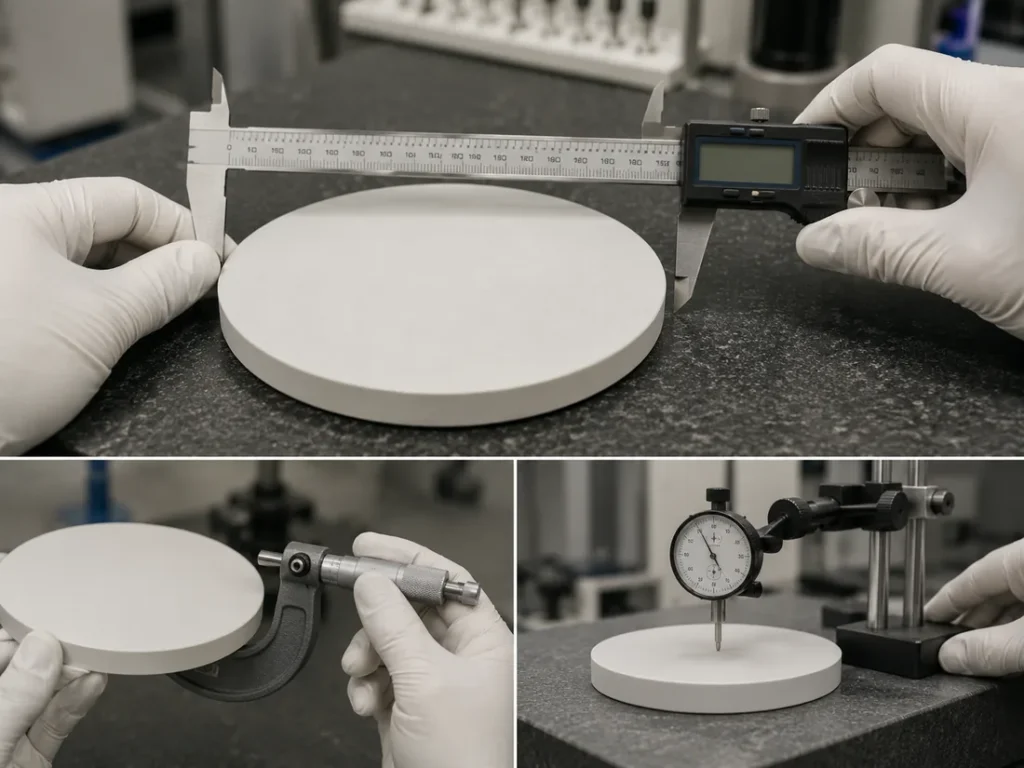
- Ceramic diameter, thickness, flatness, and edge condition
- Backing-plate diameter, thickness, holes, and PCD
- Total bonded-assembly thickness
- Target density and resistivity, when specified in the order
- Bond coverage or bonded-assembly inspection, where agreed
- Inspection against the approved drawing and acceptance criteria
Documentation & Packaging
- Order-specific Certificate of Analysis
- Dimensional inspection report
- Composition and impurity data
- Density or target-resistivity report, when specified in the order
- Bonding or assembly record, where agreed
- Lot identification and drawing-revision traceability
- Protected ceramic face, edge cushioning, and sealed packaging
Learn more about TFM’s Manufacturing Capabilities and Service & Support.
Project note: Customer-specific inspection methods, report formats, third-party testing, density or resistivity acceptance, bonding records, and special packaging requirements should be confirmed before production.
RFQ Checklist: What to Provide
| RFQ Field | Example / Information to Provide |
|---|---|
| Composition & Basis | Ga₂O₃ = 99.99% (4N) or another clearly defined ratio and basis |
| Purity | 4N / 99.99% oxide basis or customer-specific impurity limits |
| Density / Target Resistivity | Measured value, minimum acceptance criterion, or report requirement |
| Shape & Ceramic Dimensions | Disc, rectangle, step, bonded, or rotary; e.g., Ø76.2 × 3.18 mm ceramic |
| Quantity | Required pieces or complete assemblies |
| Cathode / Rotary Source | Manufacturer, model, erosion zone, active length, end geometry, or installed height |
| Bonding & Backing Plate | Unbonded or bonded; material, dimensions, holes, PCD, cooling features, and total assembly thickness |
| Power Mode & Process Gas | RF, DC, or pulsed DC; Ar, Ar/O₂, or another gas mixture |
| Operating Conditions | Maximum power, ramp rate, duty cycle, run time, and cooling |
| Film Role & Objectives | Electrode or device layer; thickness, sheet resistance, transmission range, roughness, and process temperature |
| Documentation | CoA, dimensional inspection report, composition or impurity data, density or resistivity report, bonding record, or customer-specific format |
| Drawing & Delivery | PDF, STEP, DWG, sketch, or current assembly photograph; delivery city, postal code, and country |
Minimum information required: Composition and ratio basis, purity, target dimensions, quantity, bonded or unbonded construction, cathode or rotary-source model, and a drawing or current assembly photograph.
Example RFQ
Ga₂O₃ sputtering target, Ga₂O₃ = 99.99% (4N), 4N oxide-basis purity, Ø76.2 × 3.18 mm ceramic, indium-bonded to Ø76.2 × 3.18 mm copper backing plate, total thickness 6.35 mm maximum, quantity 2 pcs. Target resistivity, CoA, and dimensional inspection report required. Please quote price, lead time, and shipping.
Frequently Asked Questions
It is used to deposit transparent conductive indium tin oxide films for displays, touch panels, photovoltaic contacts, LEDs, photodetectors, sensors, electrochromic devices, transparent heaters, and functional glass coatings.
It commonly means 90 wt% Ga₂O₃ and 10 wt% Ga₂O₃, but only when the weight-percent and oxide basis are stated. A 99.99% (4N) atomic-percent or molar-percent composition is different.
4N normally indicates 99.99% purity according to the agreed oxide or impurity basis. It does not describe the Ga₂O₃ mixing ratio or its accuracy.
Density and pore structure affect ceramic integrity, particle risk, arcing, and erosion. Target resistivity helps evaluate power-mode and plasma compatibility. They should be specified separately from film properties.
No. Film resistivity also depends on oxygen partial pressure, power, working pressure, substrate, thickness, annealing, chamber condition, and the measurement method.
Some conductive, high-density Ga₂O₃ targets can be used with DC or pulsed DC, while RF is also common. Compatibility should be confirmed from measured target resistivity, the power supply, cathode, and oxygen process.
Bonding may be selected for thin, large, brittle, or higher-load ceramic targets. The ceramic thickness, bond coverage, backing plate, cooling interface, power, and run time should be reviewed together.
Planar targets are used in planar magnetrons and are common in laboratories and many production coaters. Rotary targets are used in rotatable cathodes for large-area or continuous production and require tube, active-length, end-geometry, and cooling details.
No. The target is one process input. Final film properties depend on the complete deposition and annealing process and should be qualified on the customer’s system.
Provide composition and ratio basis, purity, target dimensions, quantity, density or resistivity requirements, bonding and backing plate, cathode model, process conditions, intended film, documentation, drawing, and delivery location.
Related Products and Resources
Request a Gallium Oxide Target Quote
Please provide the composition and ratio basis, purity, dimensions, density or resistivity requirement, bonded or unbonded construction, backing-plate drawing, cathode model, intended film, process conditions, required documentation, and delivery location.