 MSDS File
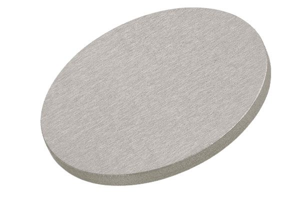
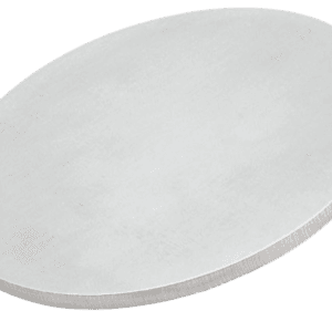
Gallium (III) Sulphide Sputtering Target Description
Gallium (III) Sulphide Sputtering Targets are highly effective in ensuring uniform and controlled thin film deposition, leading to consistent and reliable films on substrates. Known for its exceptional optical properties, Gallium Sulphide is frequently utilized in optical coatings and devices due to its favorable transmission and absorption characteristics. As a semiconductor, it provides the necessary electrical properties for the fabrication of various electronic devices. Additionally, Gallium Sulphide exhibits stability in specific environments, contributing to its long-term reliability across different applications.
Related Product: Gallium (III) Selenide Sputtering Target, CIGS Copper Indium Gallium (III) Sulphide Sputtering Target
Gallium (III) Sulphide Sputtering Target Specifications
| Compound Formula | Ga2S3 |
| Molecular Weight | 235.64 |
| Appearance | Silver Grey Target |
| Melting Point | 1255 °C |
| Density | 3.65 g/cm3 |
| Available Sizes | Dia.: 1.0″, 2.0″, 3.0″, 4.0″, 5.0″, 6.0″
Thick: 0.125″, 0.250″ |
Gallium (III) Sulphide Sputtering Target Handling Notes
Indium bonding is recommended for Gallium (III) Sulphide Sputtering Targets to address challenges related to the material’s brittleness and low thermal conductivity. Gallium (III) Sulphide has low thermal conductivity and is prone to thermal shock, making indium bonding a practical solution for maintaining stability and performance during the sputtering process.
Gallium (III) Sulphide Sputtering Target Application
Gallium (III) Sulphide Sputtering Targets are integral to various applications due to their specialized properties:
- Optical Applications: These targets are utilized in creating optical devices thanks to their distinctive optical properties. They are particularly effective in preparing transparent conductive films, optical coatings, and infrared windows.
- Electronics: As a semiconductor, Gallium Sulphide is essential for fabricating electronic components, including photodiodes and LEDs, benefiting from its electrical properties.
- Thin Film Technology: They are crucial for the thin film deposition process, ensuring the formation of uniform and reliable films on substrates. This makes them suitable for a broad spectrum of optical, electronic, and magnetic applications.
- Optical Coatings: Gallium Sulphide thin films are applied in optical coatings to enhance the material’s properties for various reflective, transmissive, and absorptive uses.
Gallium (III) Sulphide Sputtering Target Packaging
We ensure that our Gallium (III) Sulphide Sputtering Target is meticulously managed throughout storage and transportation to maintain the highest quality and integrity of the product.
Get Contact
TFM offers Gallium (III) Sulphide Sputtering Targets in various forms, purities, sizes, and prices. We specialize in high-purity thin film deposition materials with optimal density and minimal grain sizes, which are ideal for semiconductor, CVD, and PVD applications in display and optics. Contact Us for current pricing on sputtering targets and other deposition materials that are not listed.


Reviews
There are no reviews yet.