Generic selectors
Exact matches only
Search in title
Search in content
Post Type Selectors

ST0972 Germanium Phosphide Sputtering Target, GeP

Chemical Formula GeP
Catalog No. ST0972
CAS Number
Purity 99.9%, 99.95%, 99.99%, 99.995%, 99.999%
Shape Discs, Plates, Column Targets, Step Targets, Custom-made

With a commitment to excellence, TFM presents Germanium Phosphide Sputtering Targets, renowned for their unparalleled purity and competitive pricing. Drawing upon our extensive expertise in materials science, we guarantee exceptional performance and reliability through meticulous craftsmanship in the production of our targets.

MSDS File

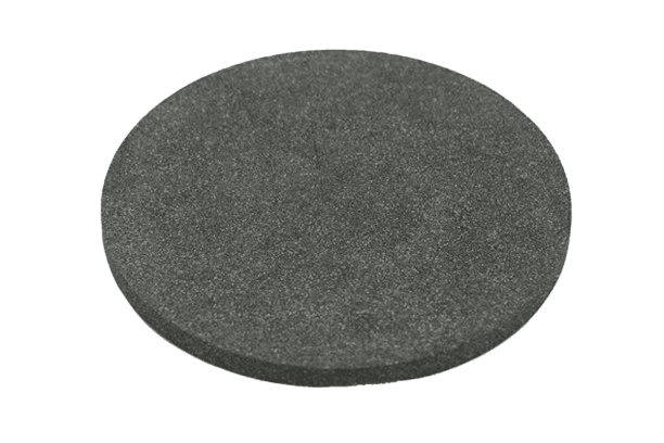
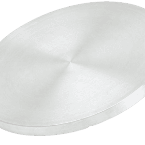
Germanium Phosphide Sputtering Target Description

Our Germanium Phosphide Sputtering Targets are engineered from top-tier materials to deliver exceptional performance and reliability. These advanced targets are designed to meet the precise demands of thin-film deposition technologies.

With their distinct Germanium Phosphide composition, these targets offer numerous advantages, including outstanding electrical conductivity, a high melting point, and remarkable chemical stability. These characteristics make them ideal for a wide range of applications, particularly in microelectronics, solar cell production, and other processes where precise material control is essential.

Whether you’re involved in cutting-edge research or advanced manufacturing, our Germanium Phosphide Sputtering Targets provide the quality and consistency you need. Our commitment to excellence ensures that these targets will enhance your thin-film deposition processes, delivering optimal results every time.

Related Product: Germanium Sputtering Target, Germanium Sulfide Sputtering Target

Germanium Phosphide Sputtering Target Specifications

Compound Formula GeP
Molecular Weight 103.61
Appearance Black Target
Melting Point 725 °C
Available Sizes Dia.: 1.0″, 2.0″, 3.0″, 4.0″, 5.0″, 6.0″

Thick: 0.125″, 0.250″

Germanium Phosphide Sputtering Target Handling Notes

Indium bonding is highly recommended for Germanium Phosphide Sputtering Targets because certain characteristics of this material, such as brittleness and low thermal conductivity, make it challenging to sputter effectively. The low thermal conductivity also makes the material prone to thermal shock, which can compromise its integrity during the sputtering process. Indium bonding helps mitigate these issues, ensuring better performance and extending the target’s lifespan.

Germanium Phosphide Sputtering Target Application

Microelectronic Manufacturing: Germanium Phosphide Sputtering Targets are integral to the production of microelectronic components. Their superior electrical conductivity makes them ideal for fabricating semiconductor devices, contributing to the development of high-performance electronics.

Photovoltaic Cells: In solar energy applications, Germanium Phosphide Sputtering Targets enhance the efficiency of photovoltaic cells. Their specific properties are crucial for optimizing solar cell performance, making them a valuable material in solar technology.

Thin Film Deposition: These targets are essential for various thin film deposition processes. Their high melting point and chemical stability ensure the formation of durable, high-quality films, particularly where precise material control is needed.

Optoelectronic Devices: Germanium Phosphide Sputtering Targets are also key in manufacturing optoelectronic devices. Their unique electrical and chemical attributes support the production of reliable components, including lasers and photodiodes, thereby boosting the performance of these devices.

Germanium Phosphide Sputtering Target Packaging

We take meticulous care in handling our Germanium Phosphide Sputtering Targets during both storage and transportation. Each target is packaged with precision to ensure it arrives in pristine condition, preserving its quality and performance throughout the delivery process.

Get Contact

TFM provides Germanium Phosphide Sputtering Targets in various forms, purities, and sizes to suit a wide range of applications. Our targets are meticulously crafted for high-purity physical vapor deposition (PVD) processes, ensuring exceptional density and minimal average grain sizes. These sputtering targets are ideal for use in semiconductor manufacturing, chemical vapor deposition (CVD), and PVD processes, as well as in display and optical applications.

Reviews

There are no reviews yet.

Be the first to review “ST0972 Germanium Phosphide Sputtering Target, GeP”

Your email address will not be published. Required fields are marked *

Related Products

FAQ

It’s the source material (in solid form) used in sputter deposition to eject atoms or molecules that then form a thin film on a substrate.

Targets can be pure metals (e.g., gold, copper, aluminum), ceramics (e.g., Al₂O₃, SiO₂, TiO₂), alloys, or composites—chosen based on the film’s desired properties.


They are produced by processes such as melting/casting for metals or sintering (often with hot isostatic pressing) for ceramics and composite targets to ensure high density and purity.


In a vacuum chamber, a plasma (typically argon) bombards the target, ejecting atoms that travel and condense on a substrate, forming a thin film.


Key factors include the target’s purity, density, grain structure, and the sputtering yield (i.e. how many atoms are ejected per incident ion), as well as operating conditions like power density and gas pressure.


Operators monitor target erosion (often by measuring the depth of the eroded “race track”) or track total energy delivered (kilowatt-hours) until it reaches a threshold that can compromise film quality.


Fragile materials (such as many ceramics or certain oxides) and precious metals often require a backing plate to improve cooling, mechanical stability, and to allow thinner targets that reduce material costs.


DC sputtering is used for conductive targets, while RF sputtering is necessary for insulating targets (like many oxides) because it prevents charge buildup on the target’s surface.


In reactive sputtering, a reactive gas (e.g., oxygen or nitrogen) is introduced to form compound films on the substrate, but it may also “poison” the target surface if not carefully controlled.


Many manufacturers prefer to control raw material quality by sourcing their own powders; using external powders can risk impurities and inconsistent target properties.


Targets should be stored in clean, dry conditions (often in original packaging or re-wrapped in protective materials) and handled with gloves to avoid contamination, ensuring optimal performance during deposition.

Deposition rate depends on factors such as target material and composition, power density, working gas pressure, substrate distance, and the configuration of the sputtering system (e.g., magnetron design).

 
Shopping Cart
Scroll to Top