Germanium Selenide Sputtering Target Description
Germanium Selenide Sputtering Targets are distinguished by their outstanding thermal stability, ensuring consistent and reliable performance during thin film deposition processes. The unique composition of Germanium Selenide enhances its exceptional electrical conductivity, making it an ideal material for applications requiring efficient charge transport.
These sputtering targets are meticulously engineered with a uniform microstructure, crucial for precision in sputtering performance. The stringent manufacturing processes involved ensure minimal impurities, thereby enhancing the overall quality of the deposited thin films.
Versatile and adaptable, Germanium Selenide Sputtering Targets are designed to meet the evolving demands of advanced technologies. Their compatibility with various sputtering systems allows for seamless integration into both research and manufacturing environments.
In summary, these sputtering targets offer high thermal stability, excellent electrical conductivity, and precise microstructural engineering, establishing them as essential materials for advanced thin film deposition technologies.
Related Product: Germanium Sputtering Target, Germanium Sulfide Sputtering Target
Germanium Selenide Sputtering Target Specifications
| Compound Formula | GeSe |
| Molecular Weight | 151.60 |
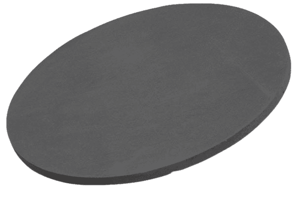
| Appearance | Black Target |
| Melting Point | 667 °C |
| Density | 5.6 g/cm3 |
| Available Sizes | Dia.: 1.0″, 2.0″, 3.0″, 4.0″, 5.0″, 6.0″ Thick: 0.125″, 0.250″ |
Germanium Selenide Sputtering Target Handling Notes
Indium bonding is recommended for Germanium Selenide Sputtering Targets due to certain characteristics that make them less suitable for sputtering on their own. Specifically, the material’s brittleness and low thermal conductivity can pose challenges during the sputtering process. The low thermal conductivity also makes the material susceptible to thermal shock. Indium bonding helps mitigate these issues by providing better thermal management and enhancing the target’s overall performance during sputtering.
Germanium Selenide Sputtering Target Application
Semiconductor Manufacturing: Germanium Selenide Sputtering Targets are essential in semiconductor manufacturing, where their excellent electrical properties make them vital for thin film deposition in semiconductor devices.
Optoelectronic Devices: The unique physical and chemical properties of Germanium Selenide make these targets critical for producing optoelectronic devices, including photovoltaic devices and various other components requiring precise thin film deposition.
Sensor Technology: Widely used in sensor manufacturing, Germanium Selenide Sputtering Targets are ideal for creating high-performance sensors due to their specialized properties.
Scientific Research: The fine control and precision offered by Germanium Selenide Sputtering Targets during thin film deposition make them valuable in scientific research and laboratory settings, where they support materials research and the development of new technologies.
Germanium Selenide Sputtering Target Packaging
Get Contact
TFM’s Germanium Selenide Sputtering Target is available in various forms, purities, and sizes. We specialize in producing high-purity physical vapor deposition (PVD) materials with the highest possible density and smallest average grain sizes, ideal for semiconductor, chemical vapor deposition (CVD), and physical vapor deposition (PVD) display and optical applications.


Reviews
There are no reviews yet.