
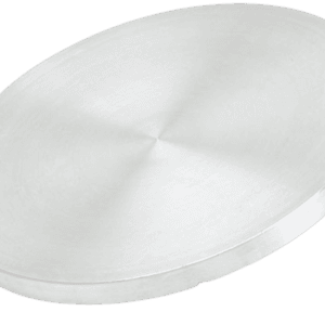
Lead Selenide Telluride Sputtering Target Description
 Lead, known as plumbum in Latin and derived from the Anglo-Saxon word for lead, has been used since around 7000 BC. It was discovered by ancient Near Eastern civilizations. Represented by the symbol “Pb” and with an atomic number of 82, lead is located in Period 6 and Group 14 of the periodic table, within the p-block. Its relative atomic mass is 207.2(1) Dalton, with the number in brackets reflecting the uncertainty of this value.
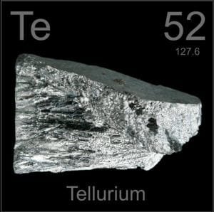 Tellurium is a chemical element named after Earth, from the Latin word *tellus*. It was first mentioned in 1782 by F.-J.M. von Reichenstein, and its isolation was later achieved and reported by H. Klaproth. The symbol for tellurium is “Te,” and it has an atomic number of 52. It is located in Period 5 and Group 16 of the periodic table, within the p-block. The relative atomic mass of tellurium is 127.60(3) Dalton, with the number in brackets representing the uncertainty.
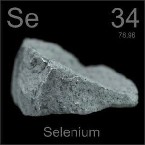
Related Products: Lead Sputtering Target, Selenium Sputtering Target, Tellurium Sputtering Target.
Lead Selenide Telluride Sputtering Target Specifications
| Material Type | Lead Selenide Telluride |
| Symbol | Pb/Se/Te |
| Color/Appearance | Gray metallic solid in various forms |
| Melting Point | / |
| Density | / |
| Available Sizes | Dia.: 2.0″, 3.0″, 4.0″, 5.0″, 6.0″ Thick: 0.125″, 0.250″ |
We also offer other customized shapes and sizes of the sputtering targets; please Contact Us for more information.
Lead Selenide Telluride Sputtering Target Application
The Lead Selenide Telluride Sputtering Target is utilized in a variety of applications including thin film deposition, decorative coatings, semiconductor fabrication, display technologies, LED and photovoltaic devices, and functional coatings. It also plays a role in the optical information storage industry, glass coating for automotive and architectural applications, and optical communication systems.
Packing
Our Lead Selenide Telluride Sputtering Targets are meticulously tagged and labeled on the exterior to guarantee easy identification and rigorous quality control. We take exceptional care to prevent any potential damage during storage and transportation, ensuring that each target reaches you in optimal condition.


Reviews
There are no reviews yet.