 MSDS File
Introduction
Lead Telluride (PbTe) Evaporation Materials are high-purity compound sources designed for precision thin film deposition in thermoelectric, infrared, and semiconductor applications. As a narrow bandgap semiconductor with excellent thermoelectric efficiency and strong infrared sensitivity, PbTe plays a critical role in mid-infrared detectors, energy harvesting modules, and advanced optoelectronic devices.
PbTe evaporation materials enable controlled deposition of stoichiometric lead telluride thin films using thermal evaporation or electron beam evaporation systems. Their stability and well-defined phase composition make them suitable for both research laboratories and industrial-scale production environments.
Detailed Description
Lead Telluride is a IV–VI compound semiconductor characterized by a direct narrow bandgap (~0.3 eV at room temperature), high carrier mobility, and low lattice thermal conductivity. These properties make it particularly valuable in thermoelectric and infrared technologies.
PbTe evaporation materials are typically manufactured through high-purity synthesis processes, including vacuum melting and controlled solidification to ensure homogeneous composition. Tight control of stoichiometry is essential, as even minor deviations in the Pb:Te ratio can significantly influence carrier concentration, Seebeck coefficient, and electrical conductivity.
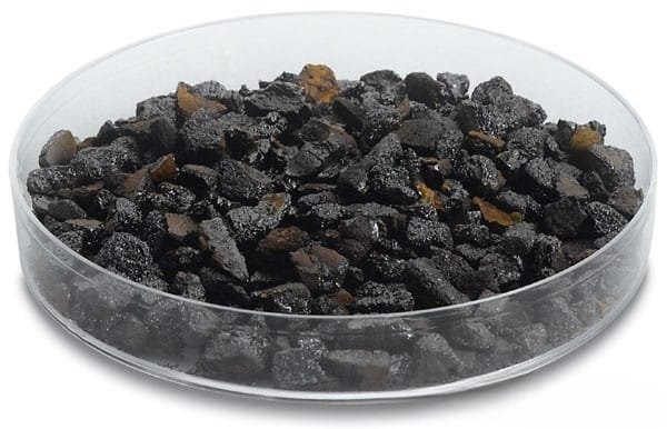
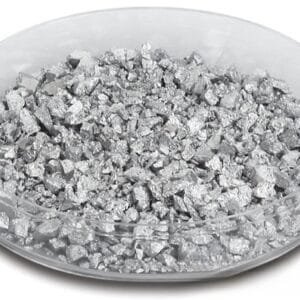
Available forms include:
Granules and lumps for resistive evaporation
Pressed tablets or pellets for stable evaporation rates
Custom-shaped pieces for e-beam crucibles
Purity levels commonly range from 99.9% to 99.999%, depending on application requirements. Low oxygen and metallic impurity levels are critical to prevent defect formation and ensure uniform film growth.
When deposited under optimized vacuum conditions, PbTe thin films exhibit:
Controlled carrier concentration
High infrared absorption in the mid-IR region
Stable thermoelectric performance
Good compatibility with multilayer semiconductor stacks
The material is particularly sensitive to temperature gradients during deposition, so controlled heating profiles are recommended to maintain stoichiometric transfer and minimize re-evaporation effects.
Applications
Lead Telluride evaporation materials are widely used in:
Thermoelectric Devices – High-efficiency power generation and cooling modules
Infrared Detectors – Mid-infrared sensing and imaging systems
Optoelectronic Components – IR photodetectors and semiconductor devices
Energy Harvesting Systems – Waste heat recovery technologies
Research & Advanced Semiconductor Studies – Band structure and quantum material investigations
PbTe remains one of the benchmark materials in thermoelectric research due to its high figure of merit (ZT) at elevated temperatures.
Technical Parameters
| Parameter | Typical Value / Range | Importance |
|---|---|---|
| Purity | 99.9% – 99.999% | Higher purity improves carrier control and film quality |
| Chemical Formula | PbTe | Ensures correct stoichiometry |
| Form | Granules / Pellets / Lumps | Compatible with thermal & e-beam systems |
| Density | ≥ 99% of theoretical | Promotes stable evaporation behavior |
| Melting Point | ~924°C | Influences evaporation method selection |
| Oxygen Content | ≤ 1000 ppm (controlled) | Reduces defect formation in films |
Comparison with Related Materials
| Material | Key Advantage | Typical Application |
|---|---|---|
| Lead Telluride (PbTe) | High thermoelectric efficiency, strong IR response | Thermoelectric modules |
| Bismuth Telluride (Bi2Te3) | High ZT at near-room temperature | Cooling modules |
| Tin Telluride (SnTe) | Lead-free alternative semiconductor | Research applications |
| Lead Selenide (PbSe) | Infrared sensitivity at different wavelengths | IR detectors |
Compared with Bi₂Te₃, PbTe offers superior performance at elevated temperatures, making it ideal for high-temperature thermoelectric applications.
FAQ
| Question | Answer |
|---|---|
| Can PbTe evaporation materials be customized? | Yes, purity, form, and pellet size can be tailored to match your evaporation system. |
| Is stoichiometry critical during deposition? | Yes, maintaining the correct Pb:Te ratio is essential for optimal electrical and thermoelectric properties. |
| Which deposition method is recommended? | Both thermal evaporation and e-beam evaporation are suitable, depending on system design. |
| What industries use PbTe most frequently? | Thermoelectric energy, infrared imaging, semiconductor research, and optoelectronics. |
| How is the material packaged? | Vacuum-sealed packaging with moisture protection and shock-resistant export cartons or wooden crates. |
Packaging
Our Lead Telluride Evaporation Materials are meticulously tagged and labeled externally to ensure efficient identification and maintain high standards of quality control. We take great care to prevent any potential damage during storage and transportation, ensuring the materials arrive in perfect condition.
Conclusion
Lead Telluride Evaporation Materials provide a reliable solution for depositing high-performance thermoelectric and infrared-sensitive thin films. With controlled stoichiometry, high purity, and stable evaporation characteristics, PbTe supports advanced applications in energy conversion and semiconductor technologies.
For detailed specifications and a quotation, please contact us at sales@thinfilmmaterials.com.


Reviews
There are no reviews yet.