
 MSDS File
Magnesium Evaporation Materials
Introduction
Magnesium Evaporation Materials are widely used as a source for thin film deposition in optical, electronic, and protective coatings. Magnesium’s low density, high reactivity, and excellent transparency to visible and infrared light make it an important material for industries such as semiconductors, optics, and energy devices. When deposited as a thin film, magnesium offers unique properties for lightweight coatings, dielectric layers, and compound films such as magnesium oxide (MgO).
Detailed Description
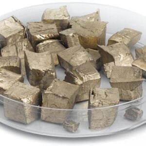
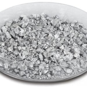
Magnesium evaporation sources are typically supplied in the form of pellets, pieces, granules, or rods, optimized for both thermal evaporation and electron beam (e-beam) evaporation systems.
Key features include:
High Purity (99.9%–99.99%): Ensures contamination-free coatings for research and industrial production.
Low Density (1.74 g/cm³): Ideal for lightweight thin film applications.
Relatively Low Melting Point (650 °C): Enables efficient evaporation under controlled conditions.
Excellent Optical Transparency: Suitable for optical coatings across UV, visible, and IR ranges.
Reactivity: Forms compounds such as MgO, useful for dielectric and protective layers.
Applications
Magnesium evaporation materials are widely applied in:
Optical Coatings: Anti-reflective and dielectric films on glass, lenses, and display panels.
Semiconductors & Microelectronics: Passivation layers and compound semiconductor thin films.
Energy Devices: Thin films for solid-state batteries, photovoltaics, and fuel cells.
Protective Coatings: Oxidation-resistant and barrier layers.
R&D: Material science experiments and nanotechnology thin film studies.
Technical Parameters
| Parameter | Typical Value / Range | Importance |
|---|---|---|
| Purity | 99.9% – 99.99% | Higher purity yields reliable thin films |
| Forms Available | Pellets, granules, rods, pieces | Compatible with various evaporation systems |
| Melting Point | 650 °C | Relatively low, suitable for efficient evaporation |
| Density | 1.74 g/cm³ | Enables lightweight thin film coatings |
| Evaporation Method | Thermal / e-beam | Provides flexibility in deposition processes |
Comparison with Related Materials
| Material | Key Advantage | Typical Application |
|---|---|---|
| Magnesium (Mg) | Lightweight, reactive, transparent | Optical & protective coatings |
| Aluminum (Al) | High reflectivity, cost-effective | Mirrors, microelectronics |
| Calcium (Ca) | High reactivity, forms stable oxides | Dielectric & optical films |
FAQ
| Question | Answer |
|---|---|
| What forms are available? | Magnesium is offered in pellets, rods, granules, or custom-shaped pieces. |
| Can purity be customized? | Yes, 99.9% and 99.99% grades are standard, higher purities available upon request. |
| How is it packaged? | Vacuum-sealed or argon-filled containers with desiccants, shipped in export-safe cartons. |
| What is the delivery time? | Typically 2–3 weeks, depending on order size and customization. |
| Which industries use it most? | Optics, semiconductors, energy, aerospace, and R&D. |
Packaging
Because magnesium is sensitive to oxidation, all evaporation materials are vacuum-sealed or inert-gas protected. Containers are clearly labeled with purity, form, and lot number to ensure traceability. Additional protective cartons or wooden crates are used for international shipment.
Conclusion
The Magnesium Evaporation Materials provide a reliable source for producing lightweight, transparent, and high-purity thin films. With excellent optical and electronic properties, magnesium remains a key evaporation material for optics, microelectronics, energy storage, and advanced R&D applications.
For detailed specifications and a quotation, please contact us at sales@thinfilmmaterials.com.

Reviews
There are no reviews yet.