
Manganese Dioxide Sputtering Target Description
Manganese Dioxide Sputtering Target is a specialized material used in sputter deposition, a technique essential for thin-film manufacturing and coating applications.
Manganese dioxide is valued for its versatility and is employed in various fields, including batteries, catalysts, and other technological applications. Utilizing a sputtering target made of manganese dioxide enables the precise customization and fine-tuning of thin films, allowing for the development of materials with specific properties tailored to diverse technological needs.
Related Product: Manganese Oxide Sputtering Target
Manganese Dioxide Sputtering Target Specifications
| Compound Formula | MnO2 |
| Molecular Weight | 86.94 |
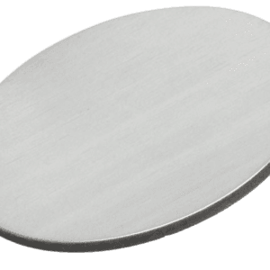
| Appearance | Black Target |
| Melting Point | >1000℃ |
| Density | – |
| Available Sizes | Dia.: 1.0″, 2.0″, 3.0″, 4.0″, 5.0″, 6.0″ Thick: 0.125″, 0.250″ |
Manganese Dioxide Sputtering Target Handling Notes
Indium bonding is recommended for the Manganese Dioxide Sputtering Target due to its inherent characteristics, such as brittleness and low thermal conductivity, which can affect the sputtering process. Manganese dioxide’s low thermal conductivity and susceptibility to thermal shock necessitate the use of indium bonding to enhance the stability and performance of the sputtering target during operation.
Manganese Dioxide Sputtering Target Application
The Manganese Dioxide Sputtering Target has diverse applications across multiple industries, including electronics, optics, and sensors. Its ability to produce thin films with specific properties makes it valuable for use in these fields and more.
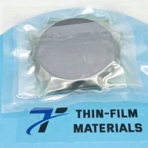
Manganese Dioxide Sputtering Target Packaging
Our Manganese Dioxide Sputtering Targets are meticulously handled during storage and transportation to ensure that they remain in optimal condition and maintain their quality.
Get Contact
TFM offers Manganese Dioxide Sputtering Targets in various forms, purities, sizes, and prices. We specialize in high-purity thin film deposition materials with optimal density and minimal grain sizes, which are ideal for semiconductor, CVD, and PVD applications in display and optics. Contact Us for current pricing on sputtering targets and other deposition materials that are not listed.

Reviews
There are no reviews yet.