
 MSDS File
Nickel Titanium Evaporation Materials
Introduction
Nickel Titanium evaporation materials are highly valued in thin film deposition for their unique combination of shape memory behavior, mechanical strength, and corrosion resistance. The alloy, commonly known as Nitinol, brings together nickel’s electrical conductivity with titanium’s strength and biocompatibility, making it an ideal choice for advanced coatings in electronics, optics, medical devices, and aerospace applications.
Detailed Description
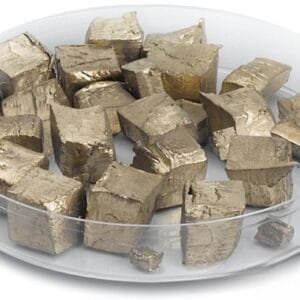
Nickel Titanium evaporation materials are produced with precise control over composition and purity to achieve stable evaporation performance and consistent film quality. Available in multiple forms such as pellets, pieces, granules, and custom shapes, these materials are optimized for both thermal and electron beam evaporation systems.
Purity: Typically available at 99.9% or higher to minimize contamination.
Composition: Standard Ni-Ti alloy ratios can be supplied, or customized according to specific thin film requirements.
Film Properties: Evaporated Ni-Ti films exhibit excellent adhesion, flexibility, and wear resistance. In certain applications, the films can retain shape memory characteristics, which is particularly useful for functional coatings.
Deposition Stability: Controlled density and particle size help prevent spitting, ensuring uniform thin film deposition.
Applications
Nickel Titanium evaporation materials are used in a wide range of industries, including:
Semiconductors – diffusion barriers and conductive layers.
Optical coatings – protective and decorative films.
Medical devices – biocompatible coatings for implants and surgical tools.
Aerospace & automotive – thin films with high fatigue resistance.
Energy devices – electrode and functional coatings in batteries and smart materials.
Technical Parameters
| Parameter | Typical Value / Range | Importance |
|---|---|---|
| Purity | 99.9% – 99.99% | High purity improves film performance |
| Forms Available | Pellets, pieces, granules, custom | Suitable for thermal and e-beam systems |
| Size Range | 1 – 20 mm (pellets/granules) | Affects evaporation uniformity |
| Evaporation Method | Thermal / Electron beam | Flexible deposition options |
| Composition | Ni-Ti alloy (customizable) | Enables tailoring of shape memory and mechanical properties |
Comparison with Related Materials
| Material | Key Advantage | Typical Application |
|---|---|---|
| Nickel Titanium (Ni-Ti) | Shape memory & biocompatibility | Medical & aerospace coatings |
| Pure Nickel | High conductivity & ductility | Electronic thin films |
| Pure Titanium | Strength & corrosion resistance | Aerospace & biomedical coatings |
| Nickel Chromium (Ni-Cr) | Oxidation resistance | Protective coatings |
FAQ
| Question | Answer |
|---|---|
| Can the Ni:Ti ratio be customized? | Yes, different Ni-Ti ratios can be supplied to match required thin film properties. |
| What deposition methods are compatible? | Compatible with both thermal and electron beam evaporation. |
| How are these materials packaged? | Vacuum-sealed in inert atmospheres with protective cartons or crates for export. |
| What industries use Ni-Ti thin films most? | Medical, aerospace, electronics, and energy storage. |
| Do the films retain shape memory effects? | In some cases, yes, depending on the alloy composition and processing conditions. |
Packaging
Nickel Titanium evaporation materials are vacuum-sealed under inert gas to prevent oxidation and contamination. For export, they are cushioned with protective foam and shipped in reinforced cartons or wooden crates with clear labeling for traceability.
Conclusion
Nickel Titanium evaporation materials provide unique advantages that go beyond conventional alloys, offering shape memory properties, durability, and excellent adhesion in thin film applications. With customizable compositions, purities, and forms, they are a reliable solution for both research and industrial manufacturing.
For detailed specifications and a quotation, please contact us at [sales@thinfilmmaterials.com].


Reviews
There are no reviews yet.