
 MSDS File
Niobium Carbide Evaporation Materials
Introduction
Niobium Carbide (NbC) Evaporation Materials are widely used in thin film deposition processes where high hardness, thermal stability, and wear resistance are required. Owing to its unique combination of refractory properties and electrical conductivity, NbC is a preferred material for creating protective, conductive, and functional coatings in advanced engineering and research applications.
Detailed Description
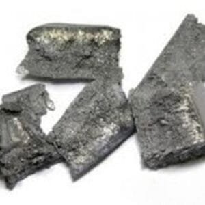
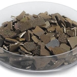
Niobium Carbide evaporation materials are typically supplied as high-purity pellets, pieces, or granules, optimized for electron beam (e-beam) and thermal evaporation systems. With a purity level of ≥99.9%, they ensure minimal contamination during deposition, providing films with consistent composition and performance.
Key features include:
High Melting Point (3500 °C) – ensures stability in high-temperature evaporation.
Hardness & Wear Resistance – suitable for protective coatings in demanding environments.
Good Electrical Conductivity – enables functional coatings for microelectronics and conductive films.
Chemical Inertness – resists oxidation and corrosion under controlled vacuum deposition.
Customizable Forms – available in pellets, tablets, or irregular pieces to match evaporation setups.
Applications
Niobium Carbide evaporation materials are used in a wide range of industries:
Semiconductors & Microelectronics – conductive films, diffusion barriers, and protective layers.
Cutting Tools & Wear-Resistant Coatings – thin films for hardness enhancement.
Aerospace & Energy – high-temperature and oxidation-resistant coatings.
Decorative Coatings – metallic-gray finish with excellent durability.
Material Science R&D – studies on refractory carbides and functional thin films.
Technical Parameters
| Parameter | Typical Value / Range | Importance |
|---|---|---|
| Purity | 99.9% (3N) | Ensures low contamination |
| Form | Pellets, pieces, granules | Matches evaporation requirements |
| Particle Size | 3 – 12 mm (customizable) | Adapts to crucible/e-beam setups |
| Melting Point | ~3500 °C | Enables high-temp thin films |
| Density | 7.82 g/cm³ | Contributes to stable evaporation rate |
Comparison with Related Materials
| Material | Key Advantage | Typical Application |
|---|---|---|
| Niobium Carbide | High hardness, thermal stability | Protective & conductive coatings |
| Titanium Carbide | Excellent wear resistance, cost-effective | Cutting tools, decorative films |
| Tantalum Carbide | Extreme thermal stability | Aerospace, ultra-high-temp films |
FAQ
| Question | Answer |
|---|---|
| What forms are available? | Pellets, tablets, granules, and custom-shaped pieces. |
| Can NbC be evaporated in standard e-beam systems? | Yes, it is suitable for both e-beam and thermal evaporation. |
| What industries benefit most from NbC films? | Electronics, aerospace, energy, cutting tools, and coating industries. |
| How is it packaged? | Vacuum-sealed with moisture protection, shipped in sturdy cartons or wooden crates. |
| Can the material be customized? | Yes, purity, size, and form can be tailored to specific deposition setups. |
Packaging
Niobium Carbide evaporation materials are carefully vacuum-sealed and moisture-protected before shipping. Each package is labeled for traceability and secured with foam inserts inside export-safe cartons or wooden crates to ensure safe transportation and storage.
Conclusion
Niobium Carbide Evaporation Materials provide exceptional performance for high-temperature, wear-resistant, and conductive thin film applications. With high purity, excellent stability, and customizable options, NbC is a reliable choice for both industrial and research-based thin film deposition.
For detailed specifications and a quotation, please contact us at [sales@thinfilmmaterials.com].

Reviews
There are no reviews yet.