 MSDS File
Introduction
Niobium Nitride Evaporation Materials (NbN) are high-performance refractory compound sources designed for thin film deposition in superconducting devices, diffusion barrier layers, and wear-resistant coatings. NbN is well known for its superconducting properties, high hardness, and chemical stability, making it a key material in quantum electronics, microelectronics, and advanced protective coatings.
Optimized for physical vapor deposition (PVD) processes such as electron beam evaporation and reactive evaporation, NbN evaporation materials enable the fabrication of uniform, high-quality nitride thin films.
Detailed Description
Niobium Nitride (NbN) is a refractory transition metal nitride with a cubic crystal structure (δ-NbN phase commonly used in superconducting applications). It exhibits:
Superconducting transition temperature (Tc) typically around 15–17 K (phase dependent)
High hardness and mechanical durability
Good chemical stability
Excellent diffusion barrier performance
NbN Evaporation Materials are manufactured using controlled nitridation and sintering processes to ensure high density and phase uniformity. Because nitrides can exhibit high melting points and strong bonding characteristics, material processing emphasizes:
High bulk density (≥95% theoretical density)
Controlled stoichiometry
Uniform microstructure
Stable evaporation behavior under high vacuum
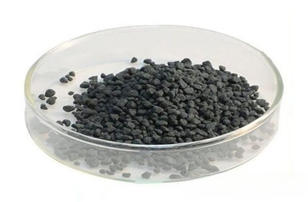
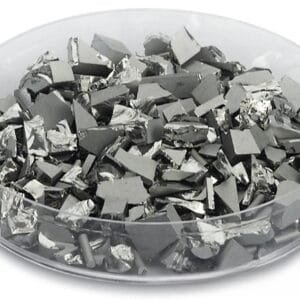
Available forms include:
Sintered ceramic pellets
Granules or broken pieces
Custom-sized feedstock for specific crucibles
For some applications, reactive evaporation using niobium metal in nitrogen atmosphere may also be employed; however, pre-compounded NbN materials provide improved stoichiometric control in certain deposition systems.
Applications
Niobium Nitride (NbN) Evaporation Materials are widely used in:
Superconducting nanowire single-photon detectors (SNSPDs)
Josephson junction devices
Quantum computing components
Diffusion barrier layers in semiconductor devices
Hard protective coatings
Microwave and RF superconducting circuits
MEMS and microelectronic structures
Wear-resistant thin films
In superconducting electronics, NbN thin films are valued for their fast response time and stable superconducting performance.
Technical Parameters
| Parameter | Typical Value / Range | Importance |
|---|---|---|
| Chemical Formula | NbN | Defines nitride phase |
| Purity | 99.9% – 99.99% | Reduces contamination |
| Density | ≥ 95% theoretical density | Stable evaporation & film uniformity |
| Form | Pellets / Pieces / Granules | Compatible with evaporation systems |
| Melting Point | > 2500°C (compound dependent) | High-temperature stability |
| Deposition Method | Electron Beam / Reactive Evaporation | Flexible processing |
Comparison with Related Materials
| Material | Key Advantage | Typical Application |
|---|---|---|
| NbN | Superconducting + hard nitride properties | Quantum & barrier films |
| TiN | High hardness & golden color coating | Decorative & barrier coatings |
| TaN | Excellent diffusion barrier | Semiconductor devices |
| Nb (metal) | Reactive nitride formation capability | Reactive PVD processes |
Compared with TiN, NbN offers superconducting functionality. Compared with TaN, NbN is particularly suited for superconducting and quantum device applications.
FAQ
| Question | Answer |
|---|---|
| Is NbN suitable for superconducting thin films? | Yes, NbN is widely used in superconducting electronics and quantum detection devices. |
| Can stoichiometry be customized? | Yes, composition adjustments can be discussed for specific deposition needs. |
| Is electron beam evaporation recommended? | Yes, e-beam evaporation is commonly used for refractory nitride materials. |
| Are small research quantities available? | Yes, flexible quantities are available for R&D applications. |
| How is the material packaged? | Vacuum-sealed, moisture-protected packaging ensures safe transport and storage. |
Packaging
Our Niobium Nitride Evaporation Materials (NbN) are meticulously tagged and labeled externally to ensure efficient identification and maintain high standards of quality control. Each batch is carefully protected to prevent contamination and mechanical damage during storage and transportation.
Conclusion
Niobium Nitride (NbN) Evaporation Materials provide a robust and high-performance source for superconducting devices, semiconductor barrier layers, and hard nitride coatings. With controlled stoichiometry, high purity, and compatibility with advanced PVD processes, NbN supports both cutting-edge quantum research and industrial thin film production.
For detailed specifications and a quotation, please contact us at sales@thinfilmmaterials.com.

Reviews
There are no reviews yet.