Confirm: Purity basis, maximum Ta/O/N/C/H limits, target dimensions, surface condition, and batch documentation.
Quick Specifications
| Item | Available Options |
|---|---|
| Material | Elemental Niobium, Nb |
| Purity | 3N–4N supply range; 3N5 and 4N commonly requested |
| Forms | Disc, rectangular, step, keeper-mounted, bonded, and custom |
| Dimensions | Standard inch sizes and custom dimensions up to approximately Ø300 mm, subject to review |
| Mounting & Bonding | Standard gun, U.S. Gun, TORUS Mag, center-hole, threaded, unbonded, or indium-bonded |
| Sputtering Process | DC, pulsed DC, RF, or reactive sputtering |
| Documentation | CoA, dimensional inspection, and agreed impurity or assembly records |
Product Overview
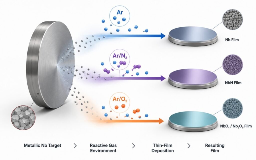
Niobium sputtering targets are used for depositing high-purity Nb thin films for superconducting, optical, and semiconductor applications. When nitrogen or oxygen is introduced during reactive sputtering, the same metallic Nb target may also be used to produce NbN or niobium oxide films.
Selection depends on film type, purity grade, target geometry, bonding method, and sputtering conditions.
Key procurement point: Specify film type (Nb / NbN / NbOx) before ordering to ensure correct target selection.
Available Niobium Target Configurations
Standard laboratory formats and drawing-specific replacement targets can be reviewed against the cathode, keeper, cooling interface, and operating conditions.
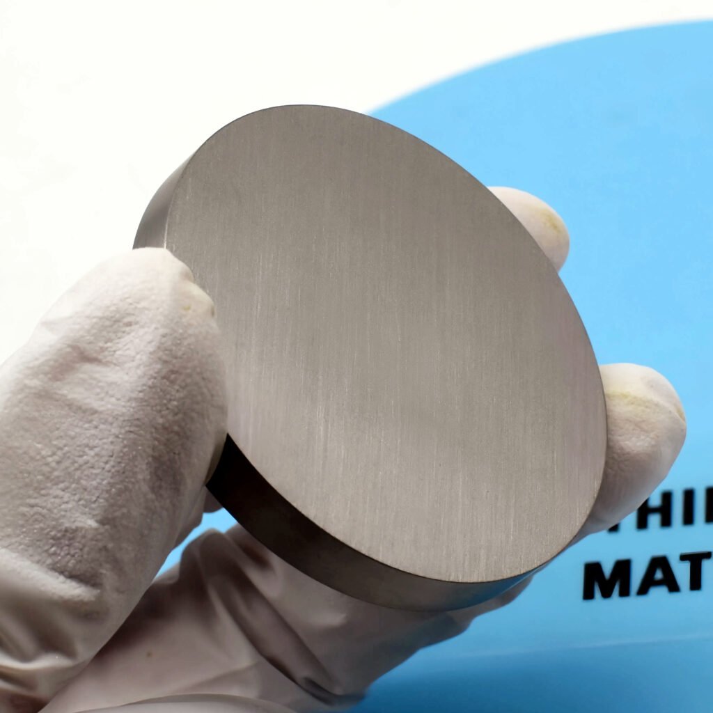
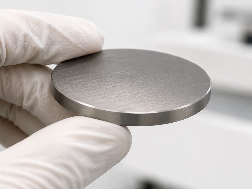
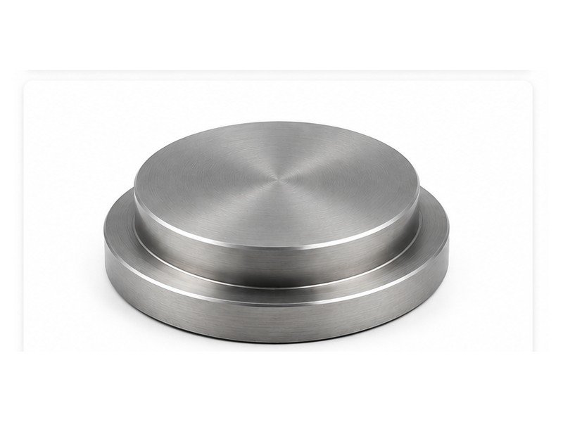
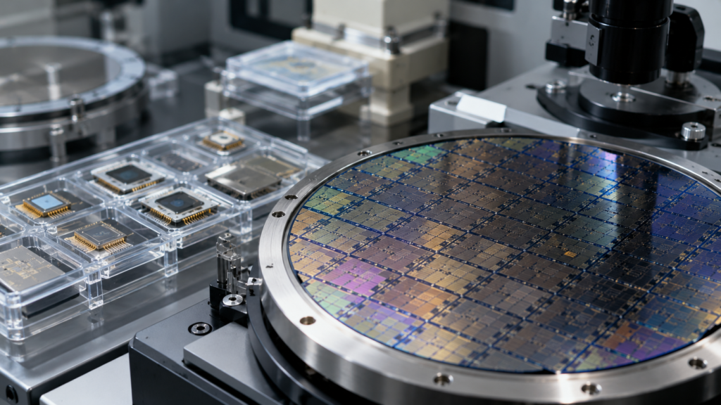
Standard Circular Targets
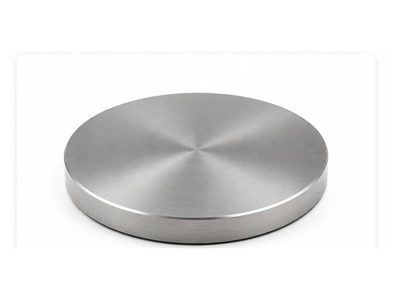
Standard discs for laboratory and production planar magnetron systems.
Keeper-Mounted / U.S. Gun Targets
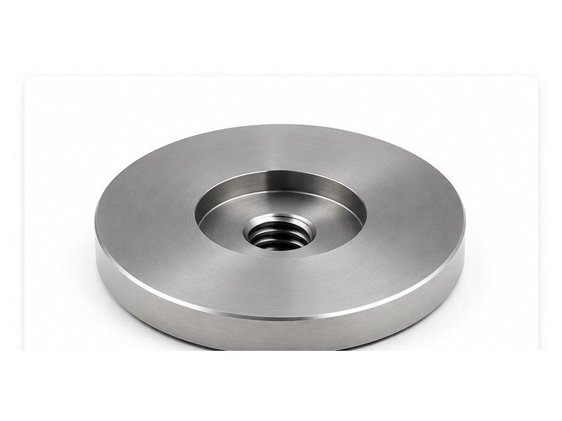
Center-hole, threaded, recessed, or keeper-compatible targets made to source geometry.
Step Targets
Shoulder and reduced-diameter designs for cathode fit and controlled installation.
Bonded Target Assemblies
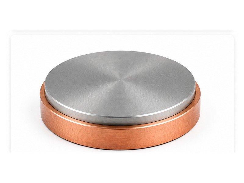
Indium-bonded targets with copper backing plates for support and heat transfer.See the Indium Target Bonding Service.
Additional Custom Target Options
TORUS Mag keeper targets, rectangular and segmented plates, center-hole or threaded targets, and
drawing-specific replacement assemblies can be reviewed. Please provide the cathode model and
current target drawing.
Niobium Sputtering Target Applications
Niobium targets support elemental Nb, reactive NbN, and niobium oxide films. Selection should follow the required film, process gas, purity, substrate, and cathode configuration.
Superconducting & Quantum Devices
Elemental Nb films for superconducting resonators, Josephson-junction structures, cryogenic circuits, and quantum-device research.
Typical projects
- Superconducting resonators
- Quantum circuits and microwave devices
- Cryogenic electronics and sensors
Niobium Nitride Thin Films
Metallic Nb targets may be reactively sputtered in Ar/N₂ to produce NbN and related nitride films.
Typical projects
- Superconducting detectors and electronics
- Nitride multilayers and sensors
- Hard coatings and material research
Confirm: Metallic Nb or a dedicated Niobium Nitride Sputtering Target, reactive-gas conditions, power mode, target dimensions, and cathode design.
Niobium Oxide Optical & Functional Films

Metallic Nb may be reactively sputtered in Ar/O₂ to produce NbOₓ or Nb₂O₅-type optical and functional films.
Typical projects
- High-index optical layers and filters
- Antireflection and dielectric coatings
- Electro-optical and sensor films
Confirm: Metallic Nb or a dedicated Niobium Oxide Target, oxygen process, substrate, optical requirements, and system configuration.
Semiconductor, MEMS & Sensor Structures
Elemental Nb conductive layers and niobium-containing multilayers for electrodes, barriers, MEMS, sensors, and prototype semiconductor devices.
Typical projects
- Conductive layers and electrodes
- Barrier and multilayer research
- MEMS and sensor structures
Confirm: Film function, impurity limits, target dimensions, layer stack, substrate temperature, cathode design, and documentation.
Explore TFM’s Semiconductor and Thin-Film Applications for additional device and coating examples.
How to Select a Niobium Sputtering Target
The target material, cathode geometry, keeper, bond, gas chemistry, power, and cooling should be selected as one complete deposition system.
| Selection Factor | What to Confirm | Why It Matters |
|---|---|---|
| Intended Film | Elemental Nb, NbN, NbOₓ, or another niobium-based film | Determines whether inert or reactive sputtering is required |
| Purity & Basis | 3N–4N range; Nb only or Nb + Ta; critical impurity limits | Impurity reporting and film requirements may differ between specifications |
| Dimensions & Cathode Fit | Diameter or L × W, thickness, step, hole, thread, recess, and installed height | Must match the cathode, cooling interface, and erosion profile |
| Mounting, Bonding & Backing Plate | Unbonded, keeper-mounted, or bonded assembly; plate dimensions and cooling features | Affects support, thermal transfer, fit, and operating limits |
| Sputtering Mode & Gas | DC, pulsed DC, RF, Ar, N₂, O₂, or mixed gas | Controls film chemistry, plasma behavior, target poisoning, and deposition rate |
| Power, Cooling & Documentation | Power, ramp rate, duty cycle, run time, cooling, CoA, and inspection scope | Supports stable operation, traceability, and acceptance |
Typical supply options range from 3N to 4N; 3N5 / 99.95% and 4N / 99.99% are commonly selected for purity-sensitive work. The total purity percentage alone does not fully determine suitability. Niobium specifications may report purity as Nb only, Nb + Ta, Nb excluding gaseous impurities, or total metallic purity. For sensitive projects, confirm whether Ta is included and specify maximum limits for Ta, O, N, C, H, and other critical impurities. Review the CoA rather than relying only on the N-grade designation.
Metallic niobium is electrically conductive and is commonly deposited using DC magnetron sputtering. Pulsed DC may be considered where additional arc control is required, while RF may be used in selected systems. Nitrogen or oxygen can change target voltage, deposition rate, arc frequency, film stoichiometry, target poisoning, process hysteresis, and gas-flow requirements. The target and reactive process should therefore be evaluated together.
A keeper-mounted target must match the source geometry. Confirm the gun model, target dimensions, center hole, thread, shoulder or recess, keeper dimensions, installed height, and cooling interface. An unbonded target may suit direct clamping or keeper mounting, while a bonded assembly may be selected for a backing plate, improved heat transfer, mechanical support, or a ready-to-install assembly. Do not assume bonded and unbonded targets can operate under identical power conditions.
Niobium Target vs Related Sputtering Materials
The correct target should be selected according to the required film chemistry, deposition route, device function, and sputtering-system configuration. These materials should not be treated as direct substitutes based only on similar refractory-metal properties.
| Material | Film & Best Suited For | When to Choose | Specifications to Confirm |
|---|---|---|---|
| Niobium, Nb | Elemental Nb films and reactively deposited NbN or NbOx; superconducting devices, quantum circuits, electrodes, and flexible reactive deposition routes. | Choose when elemental Nb is required or when NbN or NbOx will be formed by controlled reactive sputtering from a metallic Nb source. | Nb-only or Nb + Ta purity basis; Ta/O/N/C/H limits; dimensions; keeper design; bonding; power; and cooling. |
| Niobium Nitride, NbN | NbN and related nitride films for superconducting electronics, detectors, sensors, nitride multilayers, and material research. | Choose when the deposition process is qualified around a dedicated nitride target rather than reactive sputtering from metallic Nb. | Nb/N ratio; phase; purity; density; dimensions; bonding; and RF/DC compatibility. |
| Niobium Oxide | NbOx or Nb2O5-type optical, dielectric, and functional oxide films. | Choose when the process uses a direct oxide or suboxide source instead of reactive oxidation from a metallic Nb target. | Nb/O ratio; phase; purity; density; thickness; backing plate; bonding; and sputtering mode. |
| Tantalum, Ta | Ta, TaN, and TaOx films for electrodes, barriers, corrosion-resistant layers, and functional coating systems. | Choose when tantalum-specific electrical, barrier, corrosion, thermal, or device behavior is required. | Purity; phase requirement; dimensions; bonding; backing plate; and reactive-gas process. |
| Titanium, Ti | Ti, TiN, and TiOx films for adhesion layers, nitrides, oxides, barriers, and general reactive coatings. | Choose when titanium-specific adhesion, chemistry, barrier behavior, or coating performance is required. | Purity or grade; dimensions; gas chemistry; bonding; backing plate; and sputtering mode. |
Selection summary: Choose metallic Nb for elemental Nb films or flexible reactive NbN/NbOₓ deposition.
Choose a dedicated NbN or niobium oxide target when the process is qualified around a direct compound-target route. Select Ta or Ti only when their specific film chemistry or device function is required.
Custom Manufacturing, Inspection & Documentation
Custom Manufacturing
- Circular discs and rectangular plates
- Step, keeper-mounted, and custom-profile targets
- Center holes, threads, shoulders, and recesses
- Made-to-drawing unbonded or bonded assemblies
- Machined, ground, or cleaned surfaces
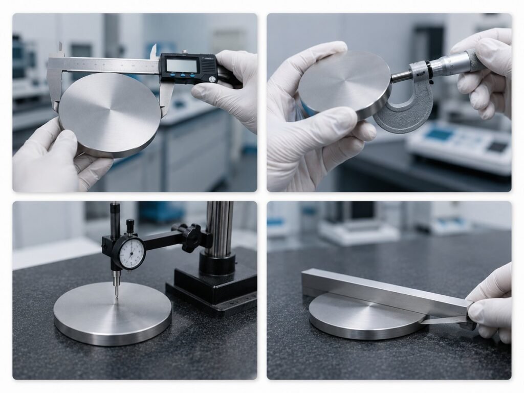
Inspection Support
- Diameter, length, width, and thickness
- Flatness and parallelism
- Surface-condition verification
- Hole, thread, recess, and keeper checks
- Bonding and assembly inspection, where agreed
- Compliance with drawings and acceptance criteria
Documentation & Packaging
- Certificate of Analysis (CoA)
- Dimensional inspection report
- Chemical composition or impurity data
- Lot and batch traceability
- Bonding or assembly records, where applicable
- Protected face and cushioned sealed packaging
Learn more about TFM’s manufacturing capabilities and Service & Support .
Project note: Customer-specific inspection methods, report formats, third-party testing, and special packaging requirements should be confirmed before production.
RFQ Checklist: What to Provide
| RFQ Field | Example / Information to Provide |
|---|---|
| Material | Niobium, Nb |
| Purity & Basis | 3N5 or 4N; state whether purity is based on Nb only or Nb + Ta |
| Critical Impurities | Maximum limits for Ta, O, N, C, H, or other project-critical elements |
| Intended Film | Elemental Nb, reactively deposited NbN, NbOₓ / Nb₂O₅, or another niobium-based film |
| Shape & Dimensions | Disc, plate, step, keeper-mounted, or custom; e.g., Ø76.2 × 6.35 mm |
| Quantity | Required quantity, e.g., 2 pcs |
| Cathode / Keeper Details | Manufacturer, model, center hole, thread, shoulder, recess, keeper profile, and installed height |
| Bonding & Backing Plate | Unbonded or bonded; backing material, dimensions, holes, PCD, and cooling features |
| Power Mode & Process Gas | DC, pulsed DC, or RF; Ar, Ar/N₂, Ar/O₂, or another gas mixture |
| Operating Conditions | Maximum power, ramp rate, duty cycle, run time, and cooling conditions |
| Documentation | CoA, dimensional inspection, impurity data, bonding record, or customer-specific reports |
| Drawing & Delivery | PDF, STEP, DWG, sketch, or current target photo; delivery city, postal code, and country |
Minimum information required: Purity, target dimensions, quantity, cathode or keeper model, bonding requirement, and a drawing or current target photograph.
Example RFQ
Niobium sputtering target, Nb 99.99%, Ø76.2 × 6.35 mm, quantity 2 pcs, unbonded, for DC magnetron deposition of superconducting Nb films. CoA and dimensional inspection report required. Please quote price, lead time, and shipping.
Niobium Target FAQ
A niobium sputtering target is used to deposit elemental Nb films and, through reactive sputtering, niobium nitride or niobium oxide films. Applications include superconducting devices, quantum research, optical coatings, semiconductors, MEMS, sensors, electrodes, and advanced thin-film development.
Standard options include 99.95% and 99.99% niobium. Other purity or impurity requirements may be reviewed. The appropriate grade depends on required film properties and limits for tantalum, oxygen, nitrogen, carbon, hydrogen, and other critical impurities.
Not necessarily. Some specifications include tantalum in the reported base-metal purity, while others report elemental niobium separately. For sensitive applications, confirm whether the stated purity is Nb only or Nb + Ta and specify the maximum acceptable tantalum content.
Yes. Metallic niobium is conductive and is commonly deposited using DC magnetron sputtering. Pulsed DC or RF may also be used depending on the equipment and process. Target mounting, cooling, power, and reactive-gas conditions should still be reviewed.
Yes. A metallic Nb target can be reactively sputtered in an argon and nitrogen atmosphere to produce NbN and related nitride films. Nitrogen flow, pressure, target poisoning, power, substrate temperature, and target condition affect the resulting film.
Yes. Niobium oxide films can be produced by reactively sputtering a metallic Nb target in an oxygen-containing atmosphere. Oxygen flow, arcing, target oxidation, deposition rate, and film stoichiometry must be controlled.
Choose metallic Nb when reactive nitrogen sputtering is part of the process or when both elemental Nb and NbN films may be required. Choose a dedicated NbN target when the deposition process is specifically designed around a compound target.
Yes. Keeper-mounted targets are available for selected standard, U.S. Gun, TORUS Mag, and drawing-specific sources. The gun model, target dimensions, hole or thread details, keeper profile, and current target drawing should be provided.
Bonded assemblies can be reviewed when improved thermal transfer, mechanical support, or backing-plate compatibility is required. Target size, bonding material, backing plate, power, cooling, and operating temperature must be evaluated together.
No. Target purity is important, but film performance also depends on the specific impurity profile, chamber base pressure, residual oxygen, substrate preparation, target conditioning, process gas, working pressure, power, deposition rate, film thickness, and substrate temperature.
Pricing depends on purity, dimensions, weight, geometry, machining features, tolerance, surface condition, keeper design, bonding, backing plate, inspection, documentation, quantity, and raw-material availability.
Related Thin-Film Materials and Applications
Request a Germanium Target Quote
Send your required purity, conductivity type, resistivity, target dimensions, quantity, backing plate, system model, operating power, and drawing for technical review.
Shopping Cart