Generic selectors
Exact matches only
Search in title
Search in content
Post Type Selectors

ST0523 Platinum Silicide Sputtering Target, PtSiH3

Chemical Formula: PtSiH3
Catalog Number: ST0523
CAS Number: 12137-83-6
Purity: 99.9%, 99.95%, 99.99%
Shape: Discs, Plates, Column Targets, Step Targets, Custom-made

Platinum Silicide sputtering target  come in various forms, purities, sizes, and prices. Thin Film Materials (TFM) manufactures and supplies top-quality sputtering targets at competitive prices.

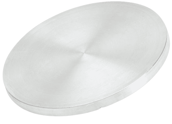
Platinum Silicide Sputtering Target Description

Platinum

Platinum Silicide (PtSi) sputtering targets are essential for thin film deposition in semiconductor, optical, and photovoltaic industries. TFM offers high-quality Platinum Silicide sputtering targets tailored to meet your specific needs and ensure precise thin-film coatings.

Related Product: Platinum Sputtering Target.

Platinum Silicide Sputtering Target Specifications

MaterialPlatinum Silicide (PtSi)
Purity99.9% and above
ShapeDiscs, Plates, or Custom Shapes
SizeDia.: 2.0″, 3.0″, 4.0″, 5.0″, 6.0″
Thick: 0.125″, 0.250″
Sputtering Target Bonding OptionsIndium, Elastomer, or Customized
Surface RoughnessAs machined or as required
Melting PointApproximately 1,890°C
Available DocumentsCertificate of Analysis (COA), MSDS, and Customized Documents
ApplicationsSemiconductor, Optical, Photovoltaic, Thin Film Coatings, and more
PackagingVacuum-sealed in plastic bags, protected by foam, and preserved in a wooden crate

We also offer other customized shapes and sizes of the sputtering targets; please Contact Us for more information.

Platinum Silicide Sputtering Target Applications

Our Platinum Silicide Sputtering Targets are suitable for a wide range of applications, including:
  • Semiconductor Device Fabrication: PtSi targets are used in the manufacturing of semiconductor devices, ensuring precise and reliable thin film coatings.
  • Optical Coatings: PtSi targets are utilized to create optical coatings for lenses, mirrors, and various optical components.
  • Photovoltaic Device Production: PtSi sputtering targets play a vital role in producing photovoltaic devices, contributing to the renewable energy sector.
  • Thin Film Deposition: PtSi is employed for thin film deposition in scientific research, enabling innovative advancements.

Packing

Our Platinum Silicide Sputtering Targets are tagged and labeled externally to ensure efficient identification and quality control. We take great care to prevent any damage during storage and transportation, preserving the quality of our products.

Reviews

There are no reviews yet.

Be the first to review “ST0523 Platinum Silicide Sputtering Target, PtSiH3”

Your email address will not be published. Required fields are marked *

Related Products

FAQ

It’s the source material (in solid form) used in sputter deposition to eject atoms or molecules that then form a thin film on a substrate.

Targets can be pure metals (e.g., gold, copper, aluminum), ceramics (e.g., Al₂O₃, SiO₂, TiO₂), alloys, or composites—chosen based on the film’s desired properties.


They are produced by processes such as melting/casting for metals or sintering (often with hot isostatic pressing) for ceramics and composite targets to ensure high density and purity.


In a vacuum chamber, a plasma (typically argon) bombards the target, ejecting atoms that travel and condense on a substrate, forming a thin film.


Key factors include the target’s purity, density, grain structure, and the sputtering yield (i.e. how many atoms are ejected per incident ion), as well as operating conditions like power density and gas pressure.


Operators monitor target erosion (often by measuring the depth of the eroded “race track”) or track total energy delivered (kilowatt-hours) until it reaches a threshold that can compromise film quality.


Fragile materials (such as many ceramics or certain oxides) and precious metals often require a backing plate to improve cooling, mechanical stability, and to allow thinner targets that reduce material costs.


DC sputtering is used for conductive targets, while RF sputtering is necessary for insulating targets (like many oxides) because it prevents charge buildup on the target’s surface.


In reactive sputtering, a reactive gas (e.g., oxygen or nitrogen) is introduced to form compound films on the substrate, but it may also “poison” the target surface if not carefully controlled.


Many manufacturers prefer to control raw material quality by sourcing their own powders; using external powders can risk impurities and inconsistent target properties.


Targets should be stored in clean, dry conditions (often in original packaging or re-wrapped in protective materials) and handled with gloves to avoid contamination, ensuring optimal performance during deposition.

Deposition rate depends on factors such as target material and composition, power density, working gas pressure, substrate distance, and the configuration of the sputtering system (e.g., magnetron design).

 
Shopping Cart
Scroll to Top