
Silicon Dioxide Sputtering Target
Introduction
Silicon Dioxide (SiO₂) Sputtering Target is one of the most widely used oxide materials for thin film deposition. Known for its excellent dielectric strength, high optical transparency, and chemical stability, SiO₂ targets are indispensable in semiconductor fabrication, optical coatings, displays, and photovoltaic devices. Thin films derived from SiO₂ provide superior insulation, passivation, and protective properties, making them essential in both industrial production and advanced R&D.
Detailed Description
Silicon Dioxide sputtering targets are produced from high-purity fused silica or quartz powders using hot pressing or vacuum sintering techniques. This ensures dense, homogeneous targets with stable sputtering performance and minimal contamination.
Chemical Formula: SiO₂
Purity: Available in 99.9% – 99.999% (3N–5N) to meet semiconductor-grade requirements.
Appearance: Transparent to translucent solid, depending on fabrication process.
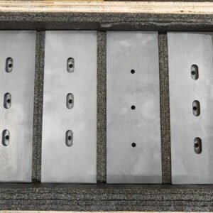
Forms & Dimensions: Circular targets (25–300 mm), rectangular plates, and custom sizes. Thickness typically ranges from 3–6 mm.
Bonding Options: Indium or elastomer bonding to copper or titanium backing plates for improved heat dissipation.
Properties: High dielectric constant, low thermal expansion, and excellent optical transmission from UV to IR.
Applications
SiO₂ sputtering targets are widely used in:
Semiconductors – Gate dielectrics, passivation layers, and insulating films.
Optical Coatings – Anti-reflective layers, beam splitters, and protective coatings.
Displays (TFT-LCD, OLED) – Transparent insulating and protective layers.
Photovoltaics – Encapsulation, passivation, and optical coatings in solar cells.
R&D – Thin film studies in electronics, photonics, and nanotechnology.
Technical Parameters
| Parameter | Typical Value / Range | Importance |
|---|---|---|
| Purity | 99.9% – 99.999% | High purity ensures semiconductor-grade films |
| Diameter | 25 – 300 mm (custom) | Compatible with most sputtering systems |
| Thickness | 3 – 6 mm | Affects sputtering stability and film thickness |
| Bonding | Copper / Titanium backing | Improves thermal management and target durability |
Comparison with Related Materials
| Material | Key Advantage | Typical Application |
|---|---|---|
| Silicon Dioxide (SiO₂) | Excellent dielectric & optical clarity | Semiconductors, optics |
| Silicon Nitride (Si₃N₄) | High hardness, good diffusion barrier | Microelectronics, coatings |
| Hafnium Oxide (HfO₂) | High-k dielectric, thermal stability | Advanced gate dielectrics |
FAQ
| Question | Answer |
|---|---|
| Can SiO₂ targets be customized? | Yes, purity, size, and bonding options are fully customizable. |
| What is the delivery time? | Standard lead time is 2–3 weeks, depending on order size and specifications. |
| Are SiO₂ targets fragile? | Yes, being a ceramic material, they should be handled carefully. |
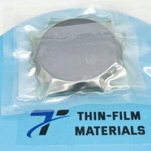
| How is it packaged? | Vacuum-sealed with protective foam in export-safe cartons or wooden crates. |
| Which industries use SiO₂ targets most? | Semiconductors, optics, display technologies, solar energy, and R&D. |
Silicon Dioxide Sputtering Target Bonding Service
Specialized bonding services for Silicon Oxide Sputtering Targets, including indium and elastomeric bonding techniques, enhance performance and durability. Thin Film Materials (TFM) ensures high-quality solutions that meet industry standards and customer needs.
We also offer custom machining of backing plates, which is essential for sputtering target assembly. This comprehensive approach improves target design flexibility and performance in thin film deposition. Our channels provide detailed information about bonding materials, methods, and services, helping clients make informed decisions.

Packaging
Silicon Dioxide Sputtering Targets are vacuum-sealed to prevent contamination and moisture absorption. Each target is carefully cushioned with protective foam and shipped in export-grade cartons or wooden crates, with clear labeling for traceability.
Conclusion
Silicon Dioxide Sputtering Targets provide outstanding dielectric, optical, and chemical stability, making them a key material in thin film deposition for semiconductors, optics, and energy devices. With high purity, customizable specifications, and reliable performance, SiO₂ targets are the preferred choice for both industrial-scale production and advanced research.
For detailed specifications and a quotation, please contact us at [sales@thinfilmmaterials.com].

Reviews
There are no reviews yet.