
Introduction
Silicon Sulfide (SiS₂) sputtering targets are specialized materials used for depositing sulfur-containing silicon thin films in advanced research and functional coating applications. As interest grows in chalcogenide-based materials for optoelectronics, solid-state devices, and infrared technologies, SiS₂ has emerged as a promising candidate due to its unique bonding structure and tunable optical properties. High-quality sputtering targets are essential to ensure compositional accuracy and stable thin film performance.
Detailed Description
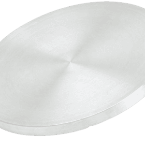
Silicon Sulfide (SiS₂) is a chalcogenide compound characterized by a chain-like molecular structure, which differentiates it from oxide-based silicon materials such as SiO₂. This structural feature contributes to its distinct optical bandgap, infrared transparency, and potential semiconducting behavior.
SiS₂ sputtering targets are typically produced through controlled synthesis and consolidation processes to ensure phase purity and uniform composition. Due to the volatile nature of sulfur and the sensitivity of SiS₂ to environmental conditions, manufacturing requires careful atmosphere control to prevent decomposition or contamination.
The target density and microstructure play a critical role in sputtering performance. High-density targets reduce particle generation and enable stable plasma conditions, while uniform grain distribution ensures consistent film deposition. Depending on system requirements, SiS₂ targets can be supplied in bonded or unbonded configurations, with copper or titanium backing plates used to improve heat dissipation during sputtering.
Applications
Silicon Sulfide Sputtering Targets are used in a range of advanced and emerging technologies:
- Chalcogenide Thin Films: For optical and electronic materials research
- Infrared Optical Coatings: Leveraging transparency in IR regions
- Semiconductor Research: Exploration of non-oxide silicon compounds
- Energy Storage & Solid-State Electrolytes: Investigating sulfur-based materials
- Photonic Devices: Thin films for waveguides and optical components
Technical Parameters
| Parameter | Typical Value / Range | Importance |
|---|---|---|
| Chemical Formula | SiS₂ | Defines compound structure |
| Purity | ≥ 99.9% (3N) | Ensures film consistency and performance |
| Density | ≥ 95% theoretical density | Improves sputtering stability |
| Diameter | 25 – 150 mm (custom) | Compatible with various sputtering systems |
| Thickness | 3 – 6 mm | Influences deposition rate and lifetime |
| Bonding | Unbonded / Cu-backed / Ti-backed | Enhances thermal management |
Comparison with Related Materials
| Material | Key Advantage | Typical Application |
|---|---|---|
| SiS₂ | Sulfur-based, IR transparency | Photonics, chalcogenide films |
| SiO₂ | Excellent dielectric properties | Insulating layers, optics |
| Si₃N₄ | High mechanical strength & stability | Protective coatings |
| GeS₂ | Broader IR transmission range | Infrared optics |
FAQ
| Question | Answer |
|---|---|
| Is SiS₂ stable during sputtering? | Yes, under controlled vacuum conditions, it can be sputtered effectively, though process parameters must be optimized due to sulfur volatility. |
| Can the target be customized? | Yes, dimensions, purity, and bonding options can be tailored to specific equipment and applications. |
| What sputtering method is recommended? | RF sputtering is typically preferred for compound ceramic materials like SiS₂. |
| How should the target be stored? | It should be stored in a dry, inert environment to prevent degradation. |
| What industries use SiS₂ targets? | Primarily research institutions, optics, and advanced semiconductor development sectors. |
Packaging
Our Silicon Sulfide Sputtering Target, SiS₂, is meticulously tagged and labeled externally to ensure efficient identification and maintain high standards of quality control. We take great care to prevent any potential damage during storage and transportation, ensuring the target arrives in perfect condition.
Conclusion
Silicon Sulfide Sputtering Targets provide a reliable solution for depositing sulfur-based silicon thin films with unique optical and electronic properties. With controlled composition, high density, and customizable configurations, they are well-suited for cutting-edge research and specialized industrial applications.
For detailed specifications and a quotation, please contact us at sales@thinfilmmaterials.com.

Reviews
There are no reviews yet.