Tantalum Silicide Sputtering Target
Introduction
The Tantalum Silicide (TaSi₂) Sputtering Target is a specialized material widely used in thin film deposition technologies. It combines the high melting point and chemical stability of tantalum with the semiconducting properties of silicon, making it highly valuable in microelectronics, thin film coatings, and advanced R&D applications.
Detailed Description
Tantalum silicide is an intermetallic compound known for its excellent thermal stability, strong electrical conductivity, and compatibility with semiconductor processes. When used as a sputtering target, it produces uniform, high-purity films that are essential for reliable device fabrication. Typical targets are fabricated through hot pressing or vacuum sintering, ensuring high density and minimal porosity to improve sputtering performance.
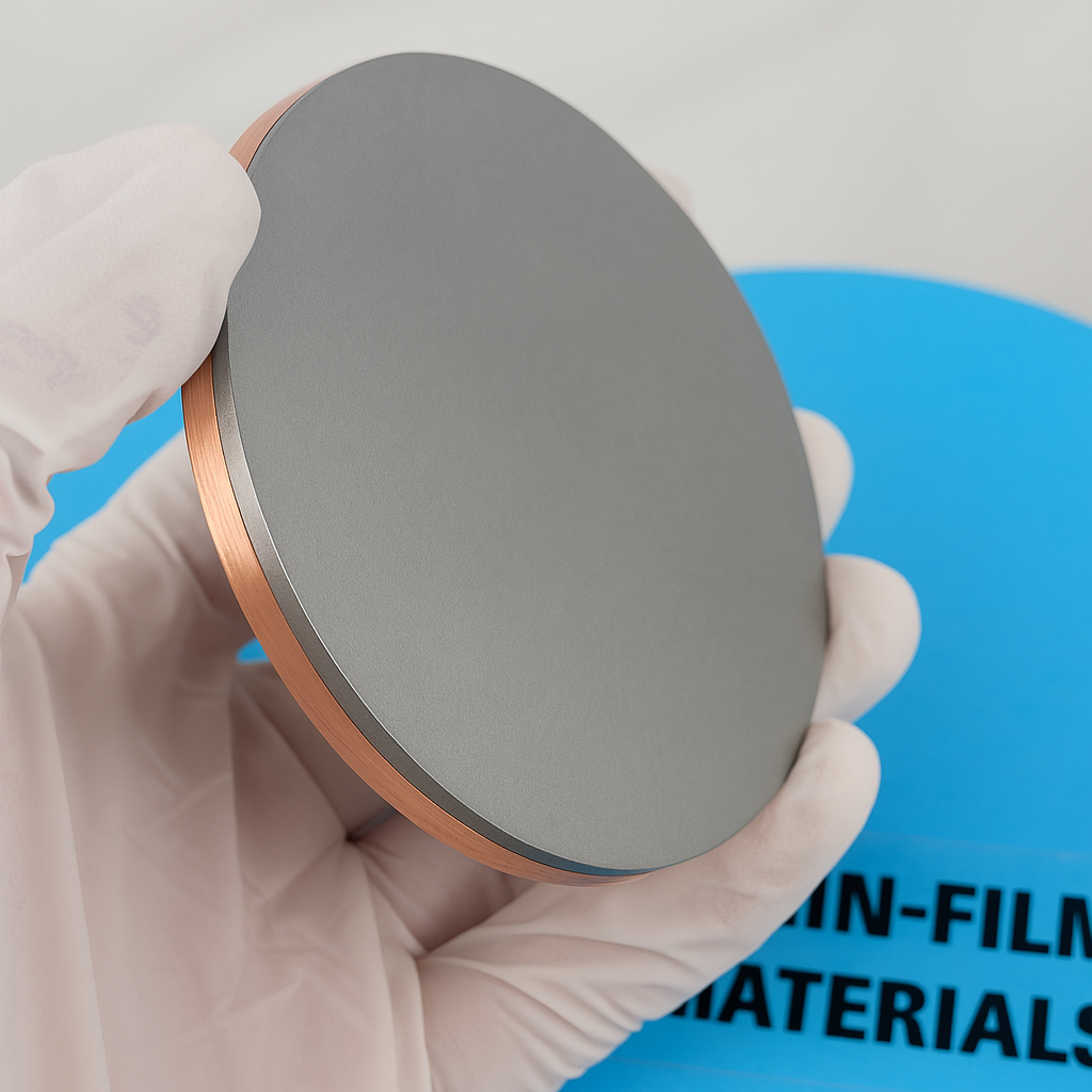
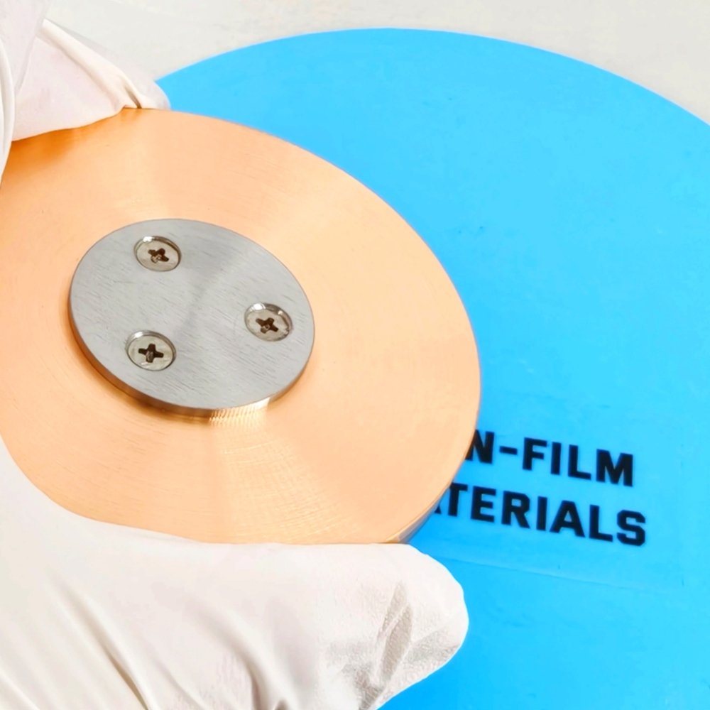
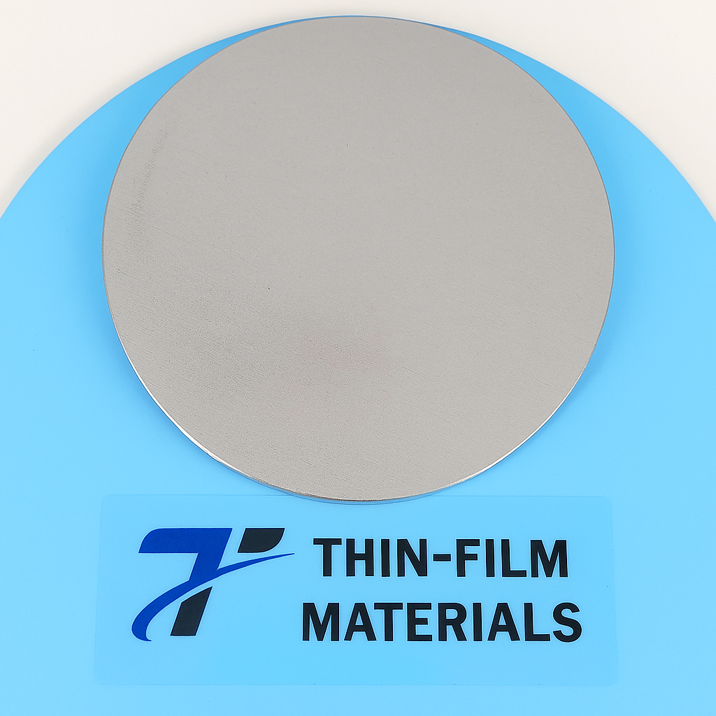
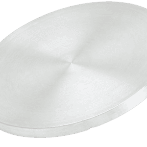
Material: TaSi₂ (Tantalum Silicide)
Purity: Available in 99.5%–99.9%
Density: ≥ 95% of theoretical density
Shape: Circular, rectangular, or custom shapes
Bonding: Elastomer or indium bonding to copper backing plates available for better heat dissipation
Applications
Microelectronics: Gate electrodes, diffusion barriers, and interconnects
Semiconductors: Thin conductive films in IC and MEMS devices
Display Technologies: Used in thin film transistor (TFT) and optoelectronic device fabrication
Research & Development: Advanced material studies in electronics, nanotechnology, and coatings
Technical Parameters
| Parameter | Typical Value / Range | Importance |
|---|---|---|
| Purity | 99.5% – 99.9% | High purity ensures reliable thin film performance |
| Density | ≥ 95% T.D. | Reduces porosity, improves film uniformity |
| Diameter | 25 – 300 mm (custom) | Fits various sputtering systems |
| Thickness | 3 – 6 mm | Affects sputtering rate and film stability |
| Bonding | Cu backing with indium/elastomer | Enhances thermal management and target life |
Comparison with Related Materials
| Material | Key Advantage | Typical Application |
|---|---|---|
| Tantalum Silicide (TaSi₂) | Excellent conductivity & high temp stability | Semiconductor interconnects, barrier layers |
| Tantalum (Ta) | Superior corrosion resistance | Capacitors, barrier layers |
| Silicon (Si) | Semiconductor compatibility | Integrated circuits, optoelectronics |
FAQ
| Question | Answer |
|---|---|
| Can the target be customized? | Yes, we provide custom sizes, shapes, and bonding options. |
| What is the delivery time? | Typically 2–3 weeks depending on quantity and specifications. |
| How are the targets packaged? | Vacuum-sealed, with protective foam in export-ready crates. |
| What bonding options are available? | Indium bonding or elastomer bonding on copper plates. |
| Which industries use TaSi₂ targets? | Mainly semiconductor, microelectronics, display, and R&D labs. |
Packaging
Each Tantalum Silicide Sputtering Target is vacuum-sealed and clearly labeled to maintain quality and traceability. Foam-lined cartons or wooden crates are used to prevent damage during storage and international transport.
Conclusion
The Tantalum Silicide (TaSi₂) Sputtering Target is a reliable material for high-performance thin film deposition, offering stability, conductivity, and compatibility with advanced semiconductor processes. With customizable specifications and strict quality control, it is an ideal choice for research institutions and industrial applications.
For detailed specifications and a quotation, please contact us at [sales@thinfilmmaterials.com].
Related Product: Tantalum Sputtering Target


Reviews
There are no reviews yet.