Tin Silver Sputtering Target Description
Tin Silver Sputtering Target is a material used in the sputtering deposition process. Sputtering is a widely used technique in thin film deposition, where atoms or ions are ejected from a solid target material and deposited onto a substrate to form a thin film.
Tin Silver Sputtering Target is often used in electronic applications, particularly in the manufacturing of solder alloys. The addition of silver to tin improves the mechanical properties, such as strength and ductility, of the solder, making it suitable for joining electronic components.
Related Product: Tin Zinc Sputtering Target, Tin Sputtering Target
Tin Silver Sputtering Target Specifications
| Compound Formula | Sn-Ag |
| Molecular Weight | 226.5 |
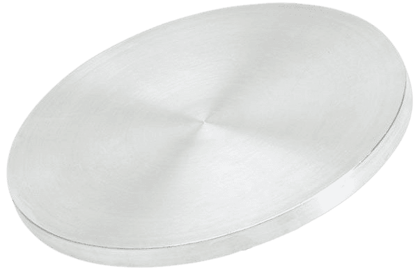
| Appearance | Silver Metallic Target |
| Available Sizes | Dia.: 1.0″, 2.0″, 3.0″, 4.0″, 5.0″, 6.0″ Thick: 0.125″, 0.250″ |
Tin Silver Sputtering Target Handling Notes
Tin Silver Sputtering Target Application
- Electronic Manufacturing: Tin Silver Sputtering Targets are crucial for producing high-performance electronic devices, thanks to their excellent electrical conductivity.
- Semiconductor Manufacturing: These targets are significant in semiconductor manufacturing, aiding in the creation of efficient and reliable semiconductor components.
- Coating Production: They play a key role in thin-film deposition processes, ensuring the production of precise and uniform coatings for various industrial and research applications.
- Nanotechnology Applications: The targets demonstrate versatility and adaptability, making them valuable in advancing nanotechnology and cutting-edge technologies.
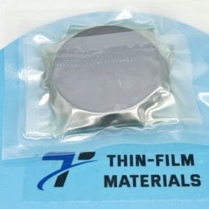
Tin Silver Sputtering Target Packaging
Our Tin Silver Sputtering Target is meticulously handled during storage and transportation to ensure the quality of our products is maintained in their original condition.
Get Contact
TFM’s Tin Silver Sputtering Target is available in various forms, purities, and sizes. We specialize in producing high-purity physical vapor deposition (PVD) materials with the highest possible density and smallest possible average grain sizes for use in semiconductor, chemical vapor deposition (CVD), and physical vapor deposition (PVD) display and optical applications.


Reviews
There are no reviews yet.