 MSDS File
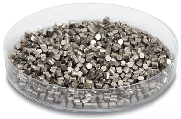
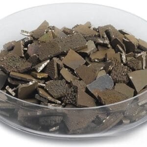
Titanium Tungsten Evaporation Materials
TFM offers high-purity titanium tungsten evaporation materials, an alloy composed of titanium (Ti) and tungsten (W). These materials are crucial in various deposition processes to ensure the production of high-quality films. Our titanium tungsten evaporation materials boast a purity level of up to 99.9995%, achieved through rigorous quality assurance procedures to ensure product reliability.
Related Products: Titanium Evaporation Materials, Tungsten Evaporation Materials
Applications of Titanium Tungsten Evaporation Materials
Our titanium tungsten evaporation materials are used in numerous applications, including:
- Deposition processes such as semiconductor deposition, chemical vapor deposition (CVD), and physical vapor deposition (PVD).
- Optics applications, including wear-resistant coatings, decorative finishes, and display technologies.
Packaging and Handling
We ensure that titanium tungsten evaporation materials are carefully tagged and labeled for easy identification and quality control. Our packaging is designed to prevent damage during storage and transportation.
Contact Us
As a leading manufacturer and supplier of high-purity titanium tungsten evaporation materials, TFM provides a range of forms including tablets, granules, rods, and wires. Customized shapes and quantities are available upon request. We also offer additional products such as evaporation sources, boats, filaments, crucibles, heaters, and e-beam crucible liners. For pricing and inquiries about our materials, including those not listed, please reach out to us directly.


Reviews
There are no reviews yet.