Introduction
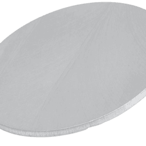
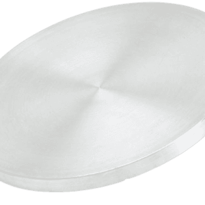
Tungsten Diboride Sputtering Target (W₂B) is an advanced ceramic compound target used in thin film deposition processes such as magnetron sputtering and other physical vapor deposition (PVD) techniques. Known for its exceptional hardness, high melting point, and outstanding chemical stability, tungsten boride materials are widely investigated for protective coatings, high-temperature applications, and advanced electronic materials.
W₂B sputtering targets enable the deposition of boride-based thin films with excellent wear resistance, thermal stability, and electrical conductivity. These properties make tungsten diboride coatings attractive for applications in cutting tools, semiconductor components, microelectronics, and high-performance protective coatings.
Detailed Description
Tungsten Diboride (W₂B) belongs to the family of transition metal borides, which are known for their remarkable combination of mechanical strength, hardness, and thermal resistance. The presence of strong covalent bonds between tungsten and boron atoms contributes to the material’s extremely high hardness and resistance to chemical attack.
Manufacturing W₂B sputtering targets typically involves advanced ceramic processing techniques. High-purity tungsten and boron precursor materials are synthesized to form the W₂B compound through high-temperature reactions. The resulting powders are then consolidated using hot pressing, vacuum sintering, or hot isostatic pressing (HIP) to achieve high-density targets suitable for sputtering applications.
High-density ceramic targets are essential for achieving stable plasma conditions and uniform sputtering rates. Dense W₂B targets reduce particle generation and improve the consistency of deposited films, which is particularly important for precision coating applications.
Thin films deposited from tungsten diboride sputtering targets often exhibit exceptional hardness, high wear resistance, and excellent thermal stability. These characteristics make W₂B coatings suitable for extreme environments where conventional coatings may fail.
Because tungsten diboride is a conductive ceramic, it can often be used in both RF and DC sputtering systems depending on the deposition configuration. For larger sputtering systems or higher power operations, targets may be bonded to copper backing plates to improve heat dissipation and mechanical stability during deposition.
Applications
Tungsten Diboride Sputtering Targets are used in a variety of advanced coating and research applications, including:
Hard protective coatings for cutting tools, molds, and wear-resistant surfaces
High-temperature coatings for components exposed to extreme thermal environments
Microelectronics and semiconductor research involving boride thin films
Electrical and conductive coatings with high thermal stability
Advanced materials research studying transition metal borides
Protective layers for aerospace and high-performance industrial components
These applications take advantage of tungsten diboride’s exceptional mechanical and thermal properties.
Technical Parameters
| Parameter | Typical Value / Range | Importance |
|---|---|---|
| Purity | 99.5% – 99.9% | Higher purity improves thin film consistency |
| Composition | Stoichiometric W₂B | Ensures proper boride film properties |
| Density | ≥ 95% theoretical density | Supports stable sputtering performance |
| Diameter | 25 – 300 mm (custom) | Compatible with various sputtering systems |
| Thickness | 3 – 6 mm | Influences sputtering rate and target lifetime |
| Bonding | Copper backing plate optional | Improves heat dissipation and structural stability |
Comparison with Related Materials
| Material | Key Advantage | Typical Application |
|---|---|---|
| Tungsten Diboride (W₂B) | Extremely hard and thermally stable boride coating | Wear-resistant and high-temperature coatings |
| Tungsten Carbide (WC) | Excellent hardness and wear resistance | Cutting tools and protective coatings |
| Titanium Diboride (TiB₂) | High hardness and good electrical conductivity | Hard coatings and conductive ceramics |
| Tungsten (W) | Very high melting point | High-temperature coatings and electronics |
FAQ
| Question | Answer |
|---|---|
| Can the Tungsten Diboride Sputtering Target be customized? | Yes, target dimensions, density, purity, and bonding options can be customized to meet specific sputtering system requirements. |
| Is W₂B a conductive material? | Tungsten diboride is considered a conductive ceramic, allowing it to be used in both RF and DC sputtering systems depending on system configuration. |
| What are the advantages of tungsten boride coatings? | They offer high hardness, excellent wear resistance, high-temperature stability, and strong chemical resistance. |
| Do W₂B targets require backing plates? | For high-power sputtering systems, copper backing plates are recommended to improve thermal conductivity and target stability. |
| Which industries use tungsten boride thin films? | Aerospace, semiconductor research, tool manufacturing, electronics, and advanced materials laboratories. |
Packaging
Our Tungsten Diboride Sputtering Target are meticulously tagged and labeled externally to ensure efficient identification and maintain high standards of quality control. We take great care to prevent any potential damage during storage and transportation, ensuring the targets arrive in perfect condition.
Conclusion
Tungsten Diboride Sputtering Targets provide a reliable material source for depositing boride-based thin films with exceptional hardness, thermal stability, and wear resistance. These coatings are valuable in demanding environments such as high-temperature applications, precision tooling, and advanced electronics research.
With customizable dimensions, high purity levels, and robust manufacturing processes, W₂B sputtering targets are designed to support modern thin film deposition systems and high-performance coating technologies.
For detailed specifications and a quotation, please contact us at sales@thinfilmmaterials.com.


Reviews
There are no reviews yet.