Generic selectors
Exact matches only
Search in title
Search in content
Post Type Selectors

VD0757 Vanadium Nitride Evaporation Materials, VN

Catalog No.VD0757
MaterialVanadium Nitride (VN)
Purity99.5%
ShapePowder/ Granule/ Custom-made

At TFM, we specialize in producing and supplying top-quality Vanadium Nitride evaporation materials known for their high purity. Our product range extends to various other evaporation materials as well. Whether you need these materials in powder or granule form, we have you covered. Additionally, we offer custom solutions to meet specific requirements, ensuring that you get exactly what you need.

Vanadium Nitride Evaporation Materials Overview

Vanadium Nitride (VN) evaporation materials, offered by TFM, are high-purity nitride ceramic compounds essential for various deposition processes. With a chemical formula of VN, these materials are crucial for producing high-quality thin films. TFM ensures exceptional reliability in its products, achieving purity levels of up to 99.9995% through rigorous quality assurance procedures.

Related Products

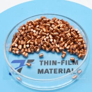
Vanadium Nitride Evaporation Materials Specification

Material TypeVanadium Nitride
SymbolVN
Appearance/ColorBlack Solid
Melting Point2,050 °C (3,720 °F; 2,320 K)
Density6.13 g/cm3
Purity99.5%
ShapePowder/ Granule/ Custom-made

Applications of Vanadium Nitride Evaporation Materials

Vanadium Nitride evaporation materials are versatile and used in:

  • Deposition Processes: Suitable for semiconductor deposition, chemical vapor deposition (CVD), and physical vapor deposition (PVD).
  • Optics: Ideal for wear protection, decorative coatings, and display technologies.

Packaging and Handling

To ensure product integrity, Vanadium Nitride evaporation materials are meticulously tagged and labeled for easy identification and quality control. Packaging is designed to prevent damage during storage and transportation.

Contact Information

TFM is a premier provider of high-purity Vanadium Nitride evaporation materials, available in various forms such as tablets, granules, rods, and wires. Custom shapes and quantities can be requested. Additionally, TFM offers evaporation sources, boats, filaments, crucibles, heaters, and e-beam crucible liners. For current pricing and inquiries about materials not listed, please contact us directly.

Reviews

There are no reviews yet.

Be the first to review “VD0757 Vanadium Nitride Evaporation Materials, VN”

Your email address will not be published. Required fields are marked *

FAQ

  • They are high‐purity substances (e.g. metals, alloys, or compounds) used in thermal or electron‐beam evaporation processes to form thin films on substrates.

  • Typically, they’re processed into a form (often ingots, pellets, or wires) that can be efficiently vaporized. Preparation emphasizes high purity and controlled composition to ensure film quality.

  • Thermal evaporation and electron-beam (e-beam) evaporation are the two main techniques, where material is heated (or bombarded with electrons) until it vaporizes and then condenses on the substrate.

  • Thermal evaporation heats the material directly (often using a resistive heater), while e-beam evaporation uses a focused electron beam to locally heat and vaporize the source material—each method offering different control and energy efficiency.

  • Key parameters include source temperature, vacuum level, deposition rate, substrate temperature, and the distance between the source and the substrate. These factors influence film uniformity, adhesion, and microstructure.

  • Evaporation generally produces high-purity films with excellent control over thickness, and it is especially suitable for materials with relatively low melting points or high vapor pressures.

  • Challenges include issues with step coverage (due to line-of-sight deposition), shadowing effects on complex topographies, and possible re-evaporation of material from the substrate if temperature isn’t properly controlled.

  • Common evaporation materials include noble metals (e.g., gold, silver), semiconductors (e.g., silicon, germanium), metal oxides, and organic compounds—each chosen for its specific optical, electrical, or mechanical properties.

  • Selection depends on desired film properties (conductivity, optical transparency, adhesion), compatibility with the evaporation process, and the final device application (semiconductor, optical coating, etc.).

  • Optimizing substrate temperature, deposition rate, and chamber vacuum are critical for ensuring that the film adheres well and forms the intended microstructure without defects.

  • Troubleshooting may involve checking the source material’s purity, ensuring stable source temperature, verifying the vacuum level, adjusting the substrate’s position or temperature, and monitoring deposition rate fluctuations.

While evaporation tends to yield very high purity films with excellent thickness control, it is limited by its line-of-sight nature. In contrast, sputtering can deposit films more uniformly on complex surfaces and is more versatile for a broader range of materials.


Shopping Cart
Scroll to Top