
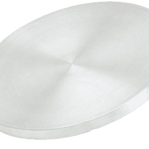
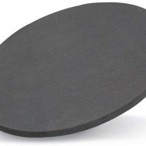
Ytterbium Fluoride Sputtering Target Description
The Ytterbium Fluoride Sputtering Target is a type of fluoride ceramic sputtering target composed of the elements ytterbium and fluorine. It is designed for use in various sputtering processes, including thin film deposition and other industrial applications.
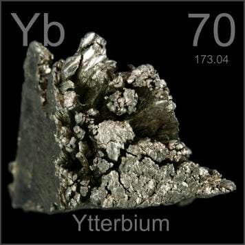 Ytterbium, symbolized as “Yb,” is a chemical element named after the village of Ytterby in Sweden. It was first identified in 1878 by J.C.G. de Marignac, with its isolation later achieved and announced by G. Urbain. Ytterbium has an atomic number of 70 and is situated in Period 6 and Group 3 of the periodic table, within the f-block. The relative atomic mass of ytterbium is approximately 173.04(3) Dalton, with the number in parentheses indicating the uncertainty of this measurement.
Related Product: Ytterbium Sputtering Target
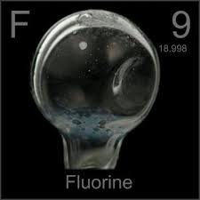 Fluorine, also known as fluorin, is a chemical element with the symbol “F.” Its name comes from the Latin word ‘fluere,’ meaning to flow. The element was first mentioned in 1810 by A.-M. Ampère, with its isolation later achieved and announced by H. Moissan. Fluorine has an atomic number of 9 and is located in Period 2 and Group 17 of the periodic table, within the p-block. The relative atomic mass of fluorine is 18.9984032(5) Dalton, with the number in brackets indicating the uncertainty of this measurement.
Ytterbium Fluoride Sputtering Target Application
The ytterbium fluoride sputtering target is used for thin film deposition, decoration, semiconductor, display, LED and photovoltaic devices, functional coating as nicely as other optical information storage space industry, glass coating industry like car glass and architectural glass, optical communication, etc.
Ytterbium Fluoride Sputtering Target Packing
Our ytterbium fluoride sputter targets are tagged and labeled externally to ensure efficient identification and quality control. Great care is taken to avoid any damage which might be caused during storage or transportation.
Get Contact
SAM’s ytterbium fluoride sputtering targets are available in various forms, purities, sizes, and prices. We specialize in producing high purity thin film coating materials with the highest possible density and smallest possible average grain sizes for use in semiconductor, chemical vapor deposition (CVD) and physical vapor deposition (PVD) display and optical applications. Please send us an inquiry for the current prices of sputtering targets and other deposition materials that are not listed.

Reviews
There are no reviews yet.