 MSDS File
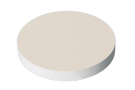
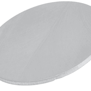
Ytterbium Oxide Sputtering Target Description
Ytterbium oxide sputtering targets from TFM are composed of the compound Yb2O3, an oxide material that includes ytterbium and oxygen. This material is utilized in various thin film deposition processes, serving applications in electronics, optics, and other advanced technology fields.
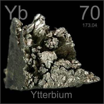 Ytterbium is a chemical element that originated from Ytterby, Sweden. It was first mentioned in 1878 and observed by J.C.G. de Marignac. The isolation was later accomplished and announced by G. Urbain. “Yb” is the canonical chemical symbol of ytterbium. Its atomic number in the periodic table of elements is 70 with a location at Period 6 and Group 3, belonging to the f-block. The relative atomic mass of ytterbium is 173.04(3) Dalton, the number in the brackets indicating the uncertainty.
Related Product: Ytterbium Sputtering Target
Oxygen, represented by the chemical symbol “O,” is a fundamental element in the periodic table with an atomic number of 8. It is located in Period 2 and Group 16, within the p-block. The name “oxygen” is derived from the Greek words ‘oxy’ and ‘genes’, meaning acid-forming. It was first identified in 1771 by the chemist W. Scheele, who also managed to isolate the element, a discovery that he announced subsequently. The relative atomic mass of oxygen is 15.9994, with the figure in brackets indicating the measurement uncertainty.
Ytterbium Oxide Sputtering Target Specification
| Compound Formula | Yb2O3 |
|---|---|
| Molecular Weight | 394.08 |
| Appearance | White |
| Melting Point | 2,355° C |
| Density | 9200 kg/m3 |
| Available Sizes | Dia.: 1.0″, 2.0″, 3.0″, 4.0″, 5.0″, 6.0″ Thick: 0.125″, 0.250″ |
Ytterbium Oxide Sputtering Target Packaging
Our ytterbium oxide sputtering target is meticulously tagged and labeled externally to facilitate easy identification and ensure stringent quality control. We take exceptional care in handling and packaging to prevent any potential damage during storage or transportation, ensuring that the product maintains its integrity and arrives in optimal condition.
Get Contact
TFM offers Ytterbium Oxide Sputtering Targets in various forms, purities, sizes, and prices. We specialize in high-purity thin film deposition materials with optimal density and minimal grain sizes, which are ideal for semiconductor, CVD, and PVD applications in display and optics. Contact Us for current pricing on sputtering targets and other deposition materials that are not listed.

Reviews
There are no reviews yet.