Generic selectors
Exact matches only
Search in title
Search in content
Post Type Selectors

ST0056 Ytterbium Sputtering Target, Yb

Chemical Formula: Yb
Catalog Number: ST0056
CAS Number: 7440-64-4
Purity: 99.9%
Shape: Discs, Plates, Column Targets, Step Targets, Custom-made

Ytterbium sputtering target  come in various forms, purities, sizes, and prices. Thin Film Materials (TFM) manufactures and supplies top-quality sputtering targets at competitive prices.

Ytterbium Sputtering Target Description

Ytterbium

The ytterbium sputtering target shares properties with its source material, ytterbium. Ytterbium is a chemical element named after Ytterby, Sweden. It was first mentioned in 1878 and observed by J.C.G. de Marignac, with its isolation later accomplished and announced by G. Urbain. The canonical chemical symbol for ytterbium is “Yb,” and it has an atomic number of 70. Ytterbium is located in Period 6 and Group 3 of the periodic table, belonging to the f-block. Its relative atomic mass is 173.04 Daltons, with the number in brackets indicating measurement uncertainty.

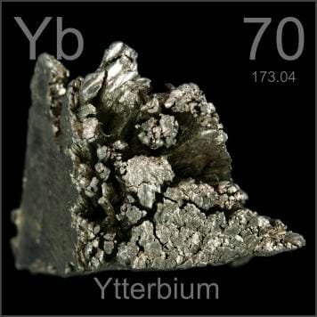
The ytterbium sputtering target is characterized by its silvery-metallic color and is often classified as a “rare-earth sputtering target.”

Ytterbium Sputtering Target Specification

Atomic Number70
Density6.90 g/cm3 (near r.t.)
Color/AppearanceSilvery White, Metallic
Thermal Conductivity34.9 W/m.K
Melting Point824 °C
Boiling Point1196 °C
Coefficient of Thermal Expansion26.3 x 10-6/K
Z Ratio1.13

Ytterbium Sputtering Target Application

Ytterbium sputtering materials are utilized in various thin-film coating applications, including:

  • CD-ROM production
  • Decorative coatings
  • Flat panel displays
  • Functional coatings
  • Optical information storage
  • Glass coatings for automotive and architectural glass
  • Optical communications

Ytterbium Sputtering Target Packaging

TFM’s ytterbium sputtering targets are clearly tagged and labeled externally to ensure efficient identification and quality control. Due to the high chemical activity of this material when exposed to the environment, we offer oil packaging and clean procedures to prevent chemical reactions and maintain the integrity of the targets.

Get Contact

TFM offers Ytterbium Sputtering Targets in various forms, purities, sizes, and prices. We specialize in high-purity thin film deposition materials with optimal density and minimal grain sizes, which are ideal for semiconductor, CVD, and PVD applications in display and optics. Contact Us for current pricing on sputtering targets and other deposition materials that are not listed.

Reviews

There are no reviews yet.

Be the first to review “ST0056 Ytterbium Sputtering Target, Yb”

Your email address will not be published. Required fields are marked *

FAQ

It’s the source material (in solid form) used in sputter deposition to eject atoms or molecules that then form a thin film on a substrate.

Targets can be pure metals (e.g., gold, copper, aluminum), ceramics (e.g., Al₂O₃, SiO₂, TiO₂), alloys, or composites—chosen based on the film’s desired properties.


They are produced by processes such as melting/casting for metals or sintering (often with hot isostatic pressing) for ceramics and composite targets to ensure high density and purity.


In a vacuum chamber, a plasma (typically argon) bombards the target, ejecting atoms that travel and condense on a substrate, forming a thin film.


Key factors include the target’s purity, density, grain structure, and the sputtering yield (i.e. how many atoms are ejected per incident ion), as well as operating conditions like power density and gas pressure.


Operators monitor target erosion (often by measuring the depth of the eroded “race track”) or track total energy delivered (kilowatt-hours) until it reaches a threshold that can compromise film quality.


Fragile materials (such as many ceramics or certain oxides) and precious metals often require a backing plate to improve cooling, mechanical stability, and to allow thinner targets that reduce material costs.


DC sputtering is used for conductive targets, while RF sputtering is necessary for insulating targets (like many oxides) because it prevents charge buildup on the target’s surface.


In reactive sputtering, a reactive gas (e.g., oxygen or nitrogen) is introduced to form compound films on the substrate, but it may also “poison” the target surface if not carefully controlled.


Many manufacturers prefer to control raw material quality by sourcing their own powders; using external powders can risk impurities and inconsistent target properties.


Targets should be stored in clean, dry conditions (often in original packaging or re-wrapped in protective materials) and handled with gloves to avoid contamination, ensuring optimal performance during deposition.

Deposition rate depends on factors such as target material and composition, power density, working gas pressure, substrate distance, and the configuration of the sputtering system (e.g., magnetron design).

 
Shopping Cart
Scroll to Top