 MSDS File
Introduction
Yttrium(III) Oxide Evaporation Materials (Y₂O₃) are high-purity rare earth oxide sources widely used in optical coatings, dielectric films, protective layers, and advanced ceramic thin film research. Y₂O₃ is valued for its high refractive index, excellent thermal stability, and strong chemical resistance, making it suitable for demanding vacuum deposition environments.
In physical vapor deposition (PVD) processes such as thermal evaporation and electron beam evaporation, material purity and stoichiometric control are critical to achieving consistent optical and electrical performance. Carefully processed Y₂O₃ evaporation materials ensure stable vaporization behavior, minimal contamination, and reliable film properties across research and industrial applications.
Detailed Description
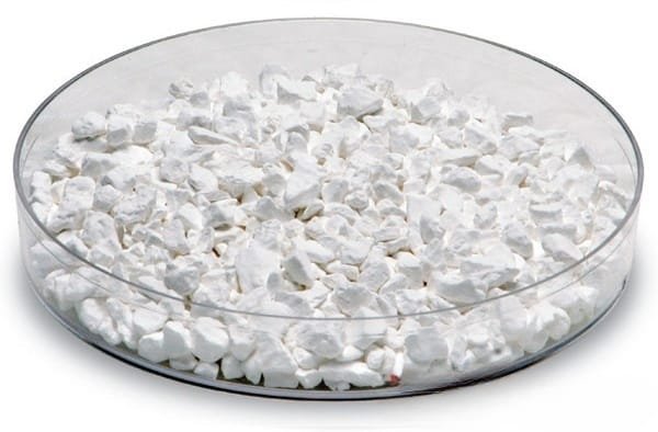
Yttrium(III) Oxide (Y₂O₃) is a white crystalline oxide with a melting point of approximately 2410°C and excellent structural stability. Its wide bandgap and strong dielectric properties make it suitable for high-performance electronic and optical thin films.
Key features include:
High Purity Grades (3N–5N typical) – Reduces trace metallic and alkali impurities that may affect dielectric strength and optical clarity.
Stoichiometric Y₂O₃ Composition – Ensures predictable film refractive index and electrical characteristics.
High Melting Point & Thermal Stability – Suitable for high-temperature deposition and post-deposition annealing.
Optimized Particle Morphology – Available in powder, granule, or pellet form to support uniform melting and controlled evaporation.
Due to its high melting temperature, electron beam evaporation is commonly preferred for Y₂O₃ deposition. Gradual power ramping is recommended to minimize spitting and ensure stable evaporation rates. In reactive or oxygen-rich environments, Y₂O₃ maintains chemical stability, making it suitable for multilayer oxide stacks.
Y₂O₃ films are often used as dielectric layers, optical high-index layers, or protective coatings in plasma and corrosive environments.
Applications
Yttrium(III) Oxide Evaporation Materials are widely used in:
Optical Coatings
High-index layers in multilayer interference filters and laser optics.High-k Dielectric Films
Gate dielectric research and advanced oxide electronics.Protective & Barrier Coatings
Plasma-resistant coatings in semiconductor processing equipment.Phosphor & Luminescent Film Research
Host matrix for rare earth-doped thin films.Advanced Ceramic Thin Films
Functional oxide layers in microelectronic and MEMS devices.
Technical Parameters
| Parameter | Typical Value / Range | Importance |
|---|---|---|
| Purity | 99.9% – 99.999% (3N–5N) | Minimizes defect density in films |
| Chemical Formula | Y₂O₃ | Ensures consistent stoichiometry |
| Melting Point | ~2410°C | Suitable for high-temperature processes |
| Refractive Index | ~1.8–1.9 (visible range) | Important for optical stack design |
| Form | Powder / Granules / Pellets | Compatible with evaporation systems |
| Packaging | Vacuum-sealed / moisture-protected | Preserves material integrity |
Comparison with Related Oxide Materials
| Material | Key Advantage | Typical Application |
|---|---|---|
| Yttrium Oxide (Y₂O₃) | High thermal stability & dielectric strength | Optical & electronic films |
| Aluminum Oxide (Al₂O₃) | Excellent hardness & insulation | Protective coatings |
| Hafnium Oxide (HfO₂) | Very high dielectric constant | Advanced gate dielectrics |
| Cerium Oxide (CeO₂) | Redox activity | Catalytic & functional films |
Compared to Al₂O₃, Y₂O₃ provides higher refractive index and improved plasma resistance. Compared to HfO₂, it offers strong dielectric properties with excellent chemical stability.
FAQ
| Question | Answer |
|---|---|
| Is Y₂O₃ suitable for thermal evaporation? | Due to its high melting point, electron beam evaporation is generally preferred. |
| Can purity levels be customized? | Yes, multiple purity grades are available depending on application requirements. |
| Does Y₂O₃ require special storage? | It is relatively stable but should be stored in dry, sealed packaging to prevent contamination. |
| What forms are available? | Powder, granules, and pellets can be supplied according to system compatibility. |
| Which industries use Y₂O₃ films most? | Semiconductor manufacturing, optics production, plasma-resistant coatings, and research institutions. |
Packaging
Our Yttrium(III) Oxide Evaporation Materials are meticulously tagged and labeled externally to ensure efficient identification and maintain high standards of quality control. We take great care to prevent any potential damage during storage and transportation, ensuring the materials arrive in perfect condition.
Conclusion
Yttrium(III) Oxide Evaporation Materials (Y₂O₃) provide a high-purity, thermally stable solution for depositing durable dielectric and optical thin films. With controlled stoichiometry, flexible supply forms, and compatibility with advanced evaporation techniques, Y₂O₃ supports demanding semiconductor, optical, and materials research applications.
For detailed specifications and a quotation, please contact us at sales@thinfilmmaterials.com.


Reviews
There are no reviews yet.