Introduction
Zinc Tin Evaporation Materials (Zn/Sn) are alloy sources developed for controlled thin film deposition in optoelectronics, transparent conducting oxides (TCOs), and functional coating systems. The Zn–Sn material system plays an important role in emerging semiconductor oxides such as zinc tin oxide (ZTO), offering tunable electrical conductivity and optical transparency.
In vacuum evaporation processes, alloy homogeneity and compositional stability directly affect the stoichiometry and performance of the resulting films. Pre-alloyed Zn/Sn evaporation materials provide reliable vapor composition, stable melting behavior, and reproducible thin film properties for both research and pilot-scale production.
Detailed Description
Zinc (Zn) is valued for its relatively low melting point and wide use in oxide electronics, while tin (Sn) contributes enhanced carrier concentration and improved structural stability in Zn-based oxide systems. When combined, Zn/Sn alloys serve as effective precursor materials for depositing mixed oxide films or metallic alloy layers.
Key characteristics include:
Pre-Alloyed Composition Control – Uniform Zn/Sn ratio ensures consistent vapor composition during evaporation.
Customizable Alloy Ratios – Typical compositions can be adjusted depending on desired electrical and optical film performance.
High Metal Purity (3N–5N typical) – Reduces unwanted impurities that could affect semiconductor properties.
Dense and Homogeneous Structure – Minimizes compositional fluctuation and particle generation.
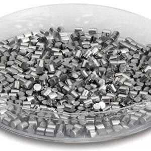
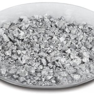
Zn/Sn evaporation materials are typically supplied as pieces, granules, or pellets compatible with tungsten boats, molybdenum crucibles, or graphite liners. Because zinc has a higher vapor pressure than tin, deposition parameters must be carefully optimized to maintain film stoichiometry.
In oxide thin film production, Zn/Sn metallic sources are often evaporated in reactive oxygen environments to form zinc tin oxide (ZTO) or related functional oxide materials.
Applications
Zinc Tin Evaporation Materials are widely used in:
Transparent Conductive Oxides (TCOs)
Precursor materials for zinc tin oxide (ZTO) thin films in displays and photovoltaics.Thin Film Transistors (TFTs)
Active semiconductor layers for next-generation display technologies.Photovoltaic Devices
Functional oxide layers in solar cell architectures.Functional & Protective Coatings
Metallic or oxide coatings with tailored conductivity and transparency.Materials Research & Development
Investigation of Zn–Sn alloy systems and oxide phase engineering.
Technical Parameters
| Parameter | Typical Value / Range | Importance |
|---|---|---|
| Purity | 99.9% – 99.999% (3N–5N) | Reduces defect density in films |
| Composition | Custom Zn/Sn ratio (wt% or at%) | Controls electrical & optical properties |
| Form | Pieces / Granules / Pellets | Compatible with evaporation systems |
| Melting Behavior | Composition-dependent (~200–420°C) | Influences evaporation control |
| Density | ≥ 99% theoretical | Promotes uniform vaporization |
| Packaging | Vacuum-sealed / inert atmosphere | Prevents oxidation |
Comparison with Related Materials
| Material | Key Advantage | Typical Application |
|---|---|---|
| Zinc Tin (Zn/Sn) | Tunable oxide semiconductor precursor | ZTO & TFT layers |
| Pure Zinc (Zn) | High vapor pressure & oxide formation capability | ZnO films |
| Pure Tin (Sn) | Improved conductivity & stability | Alloying element in TCOs |
| Indium Tin (In/Sn) | Established TCO system (ITO) | Transparent electrodes |
Compared with indium-based systems, Zn/Sn materials offer a more cost-effective and indium-free alternative for developing transparent conductive oxide films.
FAQ
| Question | Answer |
|---|---|
| Can the Zn/Sn ratio be customized? | Yes, alloy composition can be tailored to achieve target film conductivity and transparency. |
| Is the material pre-alloyed? | Yes, standard Zn/Sn evaporation materials are supplied pre-alloyed for uniform evaporation behavior. |
| Is reactive evaporation required? | For oxide film formation such as ZTO, reactive evaporation in oxygen atmosphere is typically used. |
| Are custom sizes available? | Yes, granule size and pellet dimensions can be customized based on system requirements. |
| Which industries use Zn/Sn films most? | Display manufacturing, photovoltaic development, semiconductor research, and advanced coatings R&D. |
Packaging
Our Zinc Tin Evaporation Materials are meticulously tagged and labeled externally to ensure efficient identification and maintain high standards of quality control. We take great care to prevent any potential damage during storage and transportation, ensuring the materials arrive in perfect condition.
Conclusion
Zinc Tin Evaporation Materials (Zn/Sn) provide a flexible and high-purity solution for depositing alloy and oxide thin films with tunable electrical and optical properties. With customizable composition, stable evaporation performance, and reliable packaging, Zn/Sn materials support advanced display, photovoltaic, and semiconductor applications.
For detailed specifications and a quotation, please contact us at sales@thinfilmmaterials.com.


 MSDS File


Reviews
There are no reviews yet.