Zinc Tin Oxide Sputtering Target Description
Zinc Tin Oxide (ZTO) Sputtering Targets are versatile materials used in thin film deposition processes. Comprising both zinc oxide and tin oxide, ZTO offers excellent electrical conductivity and optical transparency, making it ideal for applications in transparent conductive films, such as touchscreens, solar cells, and displays. Its notable features include high electron mobility, strong stability, and compatibility with a range of substrates. ZTO Sputtering Targets provide precise control over film thickness and composition, facilitating the production of high-performance electronic devices with improved functionality and durability.
Related Product: Zinc Sputtering Target, Tin Zinc Sputtering Target
Zinc Tin Oxide Sputtering Target Specifications
| Compound Formula | ZnO-SnO2 |
| Molecular Weight | 232.087 |
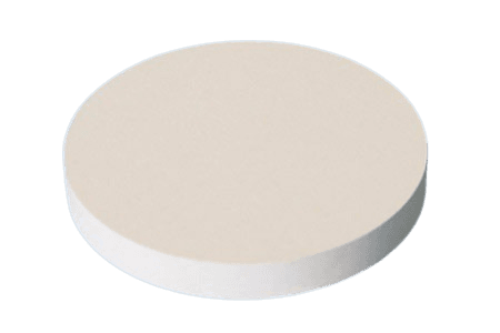
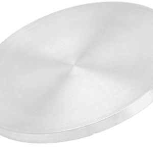
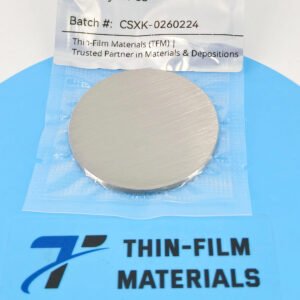
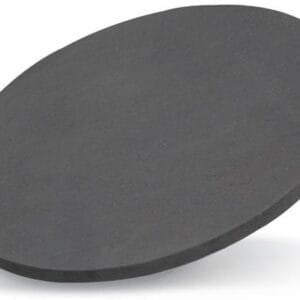
| Appearance | White Target |
| Melting Point (℃) | >570 |
| Density g/cm3 | 4.25 |
| Available Sizes | Dia.: 1.0″, 2.0″, 3.0″, 4.0″, 5.0″, 6.0″ Thick: 0.125″, 0.250″ |
Zinc Tin Oxide (ZTO) Sputtering Target Handling Notes
Zinc Tin Oxide (ZTO) Sputtering Target Application
Transparent Conductive Films: ZTO Sputtering Targets are used to deposit transparent conductive films, essential for touchscreen panels in smartphones, tablets, and other electronic devices.
Solar Cells: ZTO thin films are applied in the production of solar cells to boost their efficiency and longevity.
Displays: ZTO coatings are utilized in display technologies, including liquid crystal displays (LCDs), organic light-emitting diode (OLED) displays, and thin-film transistors (TFTs).
Smart Windows: ZTO films are integrated into smart window systems, where their conductivity can be adjusted to control light and heat transmission dynamically.
Thin-Film Transistors (TFTs): ZTO thin films function as active layers in TFTs, which are critical for flat-panel displays, sensors, and electronic circuits.
Flexible Electronics: ZTO materials are compatible with flexible substrates, making them ideal for applications in flexible electronics, such as wearable devices, flexible displays, and electronic textiles.
Reviews
There are no reviews yet.