| Material Type | ZnxCd1-xTe |
| Symbol | ZnxCd1-xTe |
| Melting Point (°C) | |
| Theoretical Density (g/cc) |
| Z Ratio | |
| E-Beam | |
| E-Beam Crucible Liner Material | |
| Temp. (°C) for Given Vap. Press. (Torr) | |
| Comments |
ZnxCd1-xTe Pellet Evaporation Material
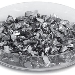
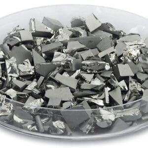
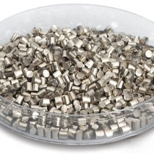
TFM offers high-quality ZnxCd1-xTe (Zinc Cadmium Telluride) pellet evaporation material, designed for thin-film deposition in advanced semiconductor and optoelectronic applications. The ZnxCd1-xTe alloy, which consists of zinc (Zn), cadmium (Cd), and tellurium (Te), is highly valued for its wide bandgap, excellent radiation detection properties, and high resistivity, making it ideal for detector technologies, infrared detectors, and solar cells.
The evaporation process using ZnxCd1-xTe pellets allows for precise control in the deposition of thin films with high purity and uniformity. These films are particularly used in the production of infrared detectors, X-ray detectors, and gamma-ray detectors, due to their high atomic number and outstanding energy resolution. ZnxCd1-xTe is also used in optoelectronic devices, where the tunable bandgap allows for customizable performance for specific light wavelength applications, such as photodetectors and laser diodes.
In addition, ZnxCd1-xTe films are used in solar energy devices, where their excellent optical properties and high electron mobility contribute to efficient energy conversion in thin-film solar cells. The material’s resistivity and structural stability make it suitable for a wide range of high-performance applications in semiconductors, imaging systems, and radiation-sensitive devices.
TFM provides customized ZnxCd1-xTe pellet evaporation materials, ensuring precise control over composition and purity to meet the specific demands of advanced thin-film deposition. These pellets are manufactured to ensure optimal evaporation performance, resulting in uniform and high-quality thin films for cutting-edge applications in infrared detection, solar energy, and optoelectronics.
The density of ZnxCd1-xTe pellet evaporation material typically ranges from 5.7 to 6.1 g/cm³, depending on the specific x value in the ZnxCd1-xTe alloy. This density range contributes to the material’s excellent thermal stability and mechanical strength, making it suitable for high-performance applications.
Our ZnxCd1-xTe pellet evaporation materials are manufactured to the highest standards, offering superior material quality, low impurity levels, and optimized evaporation characteristics. TFM’s ZnxCd1-xTe materials are perfect for advanced thin-film applications in high-tech industries, including electronics, medical imaging, and renewable energy.
The density of ZnxCd1-xTe pellet evaporation material is a key factor in its performance. With density typically ranging from 5.7 to 6.1 g/cm³, it ensures that the material maintains optimal structural integrity during deposition processes. This makes it suitable for high-tech applications, including detectors and solar energy devices.
The density of ZnxCd1-xTe pellet evaporation material plays a crucial role in ensuring uniform film formation during the evaporation process. By maintaining a density range of 5.7 to 6.1 g/cm³, TFM guarantees that the deposited films maintain high purity and uniform thickness, contributing to their superior optical and electronic properties.
The ZnxCd1-xTe pellet evaporation material‘s density is critical for applications that require precise control and performance reliability. TFM’s density-optimized ZnxCd1-xTe pellets are specifically designed to provide consistent and high-quality deposition in cutting-edge thin-film applications, from infrared sensors to solar power generation.


 MSDS File


Reviews
There are no reviews yet.