Introduction: Sputtering vs Evaporation in Thin Film Deposition
Sputtering vs evaporation is a key comparison in the world of thin film deposition. These two physical vapor deposition (PVD) methods are among the most widely used techniques for applying ultra-thin coatings in industries like semiconductors, optics, photovoltaics, and medical devices. Though both methods achieve the same goal — depositing a thin film of material onto a substrate — they differ significantly in mechanism, equipment, material compatibility, cost, and performance.
In this guide, we explore sputtering and evaporation in depth and help you decide which method is better suited for your specific application.
What is Thin Film Deposition?
Thin film deposition is the process of creating a thin layer of material on a solid surface (the substrate). The deposited layer can serve various purposes: enhancing conductivity, improving optical properties, offering protection, or forming electronic circuits.
The two most common PVD techniques are:
Each has its pros and cons, and understanding them can guide material engineers, scientists, and manufacturers to better decisions.
What is Evaporation Deposition?
Working Principle
Evaporation deposition involves heating a material until it vaporizes, then allowing the vapor to condense on a substrate, forming a thin layer. This process occurs in a high vacuum to prevent contamination and ensure directional flow of atoms.
Types of Evaporation:
- Thermal Evaporation (uses resistive heating)
- Electron Beam Evaporation (uses an electron beam for high-melting-point materials)
Steps:
- Load the material into a crucible.
- Evacuate the chamber to ultra-high vacuum.
- Heat until the material vaporizes.
- Vapor travels to the substrate and forms a thin film.
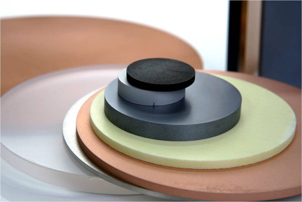
Materials Used:
- Metals: Al, Ag, Ti, Cr
- Oxides: SiO₂, Al₂O₃
- Fluorides: MgF₂, CaF₂
🡒 View Evaporation Materials at TFM
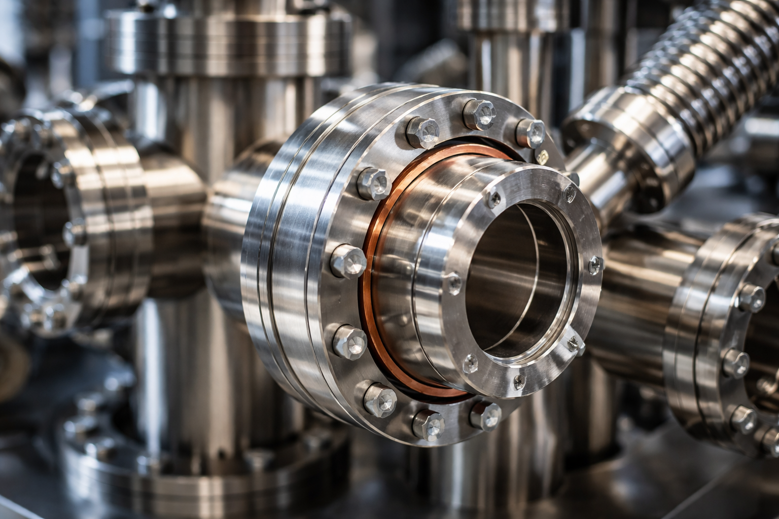
What is Sputter Deposition?
Working Principle
In sputtering, a plasma (usually argon) is used to bombard a solid target. The ions knock atoms off the target surface. These atoms then travel through the vacuum and adhere to the substrate.
Types of Sputtering:
- DC Sputtering: Ideal for conductive materials.
- RF Sputtering: Best for insulating materials.
- Magnetron Sputtering: Uses magnets to increase efficiency and uniformity.
Steps:
- Introduce argon gas into a vacuum chamber.
- Apply voltage to ionize the gas.
- Ions bombard the target.
- Ejected atoms deposit onto the substrate.
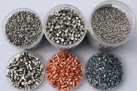
Materials Used:
- Pure Metals: Ni, Cu, Mo, Cr
- Compounds: ZnO, TiN, AlN
- Alloys: NiFe, TiAl
🡒 Explore Sputtering Targets at TFM
Sputtering vs Evaporation: Side-by-Side Comparison
| Feature | Sputtering | Evaporation |
|---|---|---|
| Energy Source | Plasma | Thermal or E-Beam |
| Vacuum Level | High (~10⁻³ to 10⁻⁶ Torr) | Ultra-high (~10⁻⁵ to 10⁻⁷ Torr) |
| Film Uniformity | Excellent | Moderate |
| Step Coverage | Good | Poor |
| Material Range | Broad | Limited by melting point |
| Deposition Rate | Slower | Faster |
| Equipment Cost | Higher | Lower |
| Adhesion Strength | Stronger | Weaker |
| Repeatability | High | Lower |
| Process Control | Precise | Moderate |
Pros and Cons of Sputtering
Advantages:
- Deposits metals, alloys, ceramics, and dielectrics
- Low substrate temperature needed
- Great uniformity on complex shapes
- Strong adhesion
- High repeatability and process control
Disadvantages:
- Slower deposition rates
- Higher equipment and maintenance cost
- Plasma may cause substrate damage in sensitive materials
Pros and Cons of Evaporation
Advantages:
- Simple and cost-effective equipment
- High deposition rates
- Suitable for high-purity materials
- Minimal substrate damage
Disadvantages:
- Poor step coverage
- Limited to materials with low-to-medium melting points
- Films may be less dense or adhesive
Use Cases: Where Each Method Excels
Evaporation is Ideal For:
- Optical Coatings (mirrors, AR coatings)
- Decorative Coatings (watch dials, plastics)
- Low-volume R&D labs
- OLEDs and Organic Films
Sputtering is Ideal For:
- Semiconductors and ICs
- Touch Panels and Displays
- Hard Coatings on Tools
- Medical Device Surfaces
- Thin-Film Batteries and Solar Cells
Which One is Better: Sputtering or Evaporation?
The best process depends on your application. Here’s a quick decision matrix:
| Application Need | Recommended Process |
|---|---|
| Cost-effectiveness | Evaporation |
| Complex materials | Sputtering |
| Superior adhesion | Sputtering |
| High throughput | Evaporation |
| Uniformity and coverage | Sputtering |
| Experimental coatings | Evaporation |
| Repeatability | Sputtering |
Industry Trends: Sputtering vs Evaporation
- Sputtering is expanding in microelectronics and energy storage.
- Evaporation is maintaining relevance in optics and decorative industries.
- Hybrid machines combining both processes are gaining traction.
- AI and machine learning are being used for better process control in both methods.
Frequently Asked Questions
Q1: Which is more environmentally friendly, sputtering or evaporation?
A: Both are relatively clean, but sputtering tends to produce less waste.
Q2: Can I deposit multiple layers with either method?
A: Yes, multilayer coatings are possible, especially with sputtering due to easier material changeover.
Q3: Which is better for complex 3D geometries?
A: Sputtering, because of its better step coverage.
Q4: Is one method more scalable than the other?
A: Sputtering is generally more scalable for industrial applications.
Q5: Which offers higher film purity?
A: Electron beam evaporation tends to produce the highest purity films.
Conclusion: Final Thoughts on Sputtering vs Evaporation
The sputtering vs evaporation debate is not about which is universally better, but which is better for your application. If you prioritize speed and low cost, evaporation is often the way to go. If you need high precision, strong adhesion, and a wide material choice, sputtering is the superior method.
For high-performance sputtering targets and evaporation materials, check out ThinFilmMaterials.com — your trusted source for deposition materials with high purity, excellent custom support, and fast global delivery.