1. Introduction: The Strategic Importance of Niobium
In the hierarchy of refractory metals, Niobium (Nb) occupies a position of unique strategic importance. While metals like Tungsten and Tantalum are prized for their extreme heat resistance, Niobium provides a versatile balance of superconductivity, biocompatibility, and chemical stability.
For the thin film industry, Niobium is not merely a coating; it is a functional enabler. As we transition into the era of quantum supremacy and advanced micro-electromechanical systems (MEMS), the demand for high-purity Niobium evaporation materials has surged. This guide provides a 360-degree view of why Niobium matters, how it behaves during Physical Vapor Deposition (PVD), and how Thin Film Materials (TFM) ensures the highest yield for global manufacturers.
2. Fundamental Material Science of Niobium (Nb)
To master the evaporation of Niobium, one must first understand its metallurgical DNA.
2.1 Atomic and Thermal Characteristics
Niobium is a soft, grey, crystalline transition metal. Its position in the periodic table (Group 5, Period 5) grants it a high melting point of 2477°C and a boiling point of 4744°C.
- Density: $8.57 g/cm^3$
- Crystal Structure: Body-Centered Cubic (BCC)
- Thermal Conductivity: $53.7 W/(m \cdot K)$ at 300 K
2.2 The Superconducting Powerhouse
Niobium’s most celebrated property is its superconductivity. It has the highest critical temperature ($T_c$) of all elemental superconductors ($9.25 K$) and the highest magnetic penetration depth. This makes Niobium thin films the “gold standard” for fabricating superconducting circuits and qubits.
3. Niobium Evaporation Techniques: Thermal vs. E-Beam
Depositing Niobium requires overcoming its high melting point and its aggressive nature as a “getter” for residual gases.
3.1 Thermal Evaporation Challenges
While thermal evaporation is the simplest PVD method, Niobium poses significant risks:
- Alloying Risk: At the temperatures required for Nb sublimation, it often reacts with the evaporation boat (typically Tungsten or Tantalum), leading to boat failure and film contamination.
- Power Constraints: Most resistive heating systems struggle to reach the stable vapor pressure required for consistent Nb deposition.
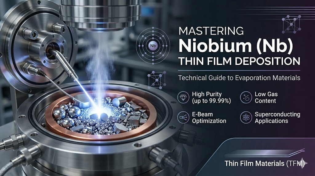
3.2 Electron Beam (E-Beam) Evaporation: The Preferred Method
E-beam evaporation is the industry standard for Niobium. By focusing a high-energy kinetic beam of electrons onto the Niobium source, the material is heated locally.
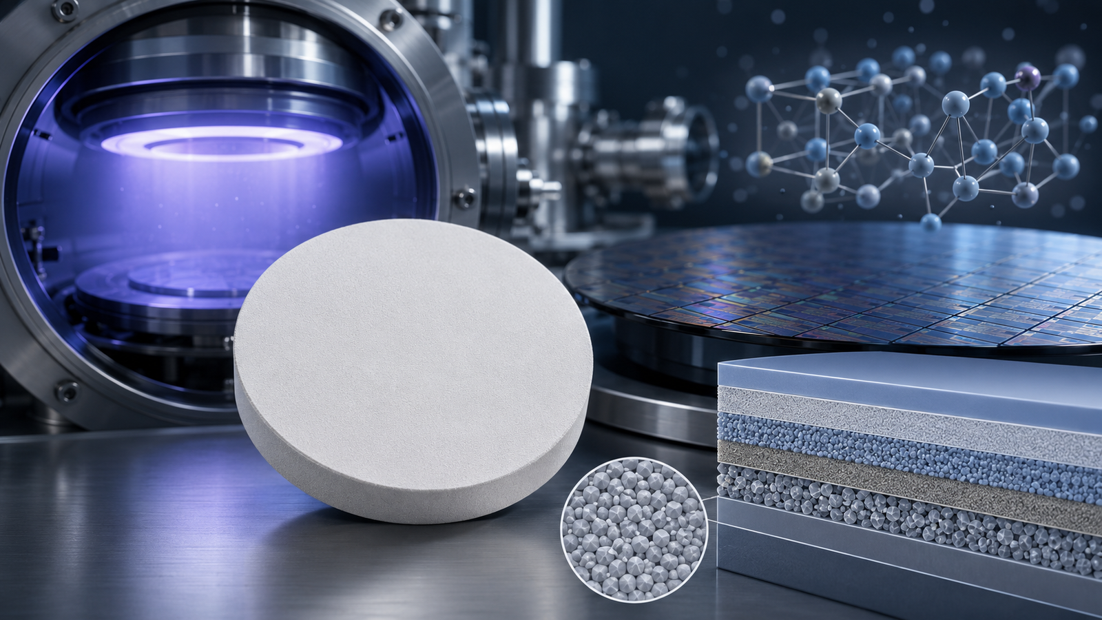
- Crucible Selection: TFM recommends using water-cooled copper hearths with high-purity Niobium “starter sources” or liners (Intermetallic or Graphite) to prevent thermal loss.
- Deposition Rate: E-beam allows for precise control over the deposition rate, ranging from $0.1 \text{\AA}/s$ to over $10 \text{\AA}/s$, depending on the application.
4. The Critical Role of Purity and Gas Content
In B2B procurement, “99.9%” is often not enough. For Niobium, the type of impurity is as important as the percentage.
4.1 Interstitial Impurities (O, N, H, C)
Niobium acts as a vacuum pump during the evaporation process. It readily absorbs Oxygen ($O_2$) and Nitrogen ($N_2$).
- The Impact: If the Niobium evaporation pellets contain high initial oxygen levels, the resulting film will have a lower $T_c$ (Critical Temperature) and higher electrical resistivity.
- TFM Solution: Our Niobium materials undergo multiple Vacuum Electron Beam Melting (VBM) cycles to drive gas content to the parts-per-million (ppm) level.
4.2 Metallic Impurities
Trace amounts of Tantalum (Ta) are common in Niobium due to their geological proximity. For high-frequency superconducting applications, TFM offers specialized low-Ta grades to ensure minimal signal loss in microwave circuits.
5. Niobium in Quantum Computing and Superconductivity
The “Quantum Gold Rush” has placed Niobium at the center of the technology map.
5.1 Josephson Junctions
The building block of a superconducting qubit is the Josephson Junction, typically a trilayer structure (e.g., Nb/Al-Oxide/Nb). The quality of the Niobium evaporation material directly correlates with the “coherence time” of the qubit.
5.2 SQUIDs and Particle Accelerators
Superconducting Quantum Interference Devices (SQUIDs) rely on the extreme sensitivity of Nb thin films to magnetic fields. Similarly, superconducting radio-frequency (SRF) cavities used in particle accelerators are often coated with Niobium to minimize energy loss.
6. Optical and Decorative Applications
Beyond the lab, Niobium is a workhorse in the optical industry.
6.1 High-Refractive Index Layers
Niobium Pentoxide ($Nb_2O_5$) films, created by reactive evaporation of Niobium in an oxygen-rich atmosphere, provide a high refractive index ($n \approx 2.3$) and excellent transparency. These are used in:
- Anti-reflective (AR) coatings.
- Optical bandpass filters.
- Smart glass applications.
6.2 Anodic Coloration
Niobium thin films can be anodized to produce a spectrum of vibrant, durable colors without the use of pigments. This is highly valued in the luxury electronics and medical device industries for identification and aesthetics.
7. Selecting the Right Form Factor: Pellets, Wire, and Rods
The geometry of your evaporation source affects your “throw distance” and material utilization.
- Evaporation Pellets (3x3mm or 6x6mm): Ideal for small R&D crucibles. They provide high surface area for rapid melting.
- Starter Sources: Pre-melted slugs designed to fit specific E-beam hearths (e.g., Temescal or Telemark). These reduce “spitting” and startup time.
- Niobium Wire: Used in continuous feed systems for high-volume industrial web coating.
8. Troubleshooting Niobium Deposition Issues
8.1 “Spitting” During Evaporation
If Niobium is not properly degassed or if it contains internal voids, it may “spit” or eject macro-particles onto the substrate.
- Fix: Ensure you are using TFM’s vacuum-melted, high-density starter sources and implement a “soak” period where the beam sweeps the material at low power before opening the shutter.
8.2 Film Stress and Adhesion
Nb films can develop high internal stress.
- Fix: Optimize the substrate temperature (typically $200°C$ to $400°C$) and use Ion-Assisted Deposition (IAD) to densify the film.
9. The TFM Manufacturing Advantage
Why do global research labs and Fortune 500 manufacturers choose Thin Film Materials (TFM)?
- Vertical Integration: We control the process from raw ore to final vacuum-melted product.
- Unrivaled Analytical Testing: Every batch is accompanied by a Certificate of Analysis (COA) detailing GDMS (Glow Discharge Mass Spectrometry) results.
- Customization: Whether you need a 5N purity for a quantum lab or a cost-effective 3N5 grade for decorative coating, we tailor the chemistry to your budget and specs.
- Sustainability: We implement closed-loop recycling for Niobium scrap, reducing environmental impact and lowering costs for our long-term partners.
10. Conclusion: Partnering for the Future of Thin Films
Niobium is more than just an element; it is the bridge to the next generation of computing, energy, and medicine. However, the sensitivity of Niobium to its environment means that your choice of evaporation material is the most critical variable in your PVD process.
At TFM, we don’t just sell materials; we provide technical partnerships. Our Niobium evaporation materials are designed to give you higher yields, fewer defects, and the peace of mind that your thin films will perform exactly as engineered.