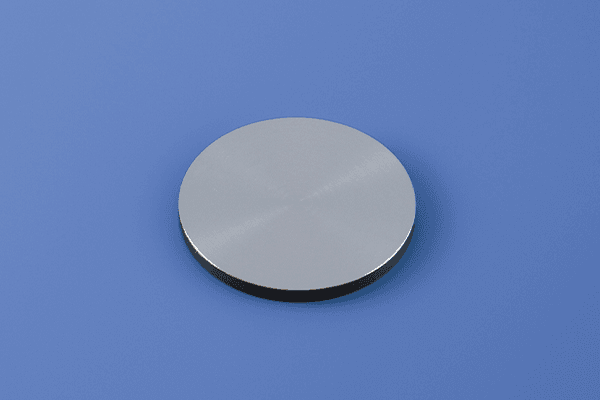
In the fast-evolving field of thin film deposition, the precision of materials used often dictates the outcome of entire technologies. Whether it’s for semiconductor devices, optical coatings, solar panels, or advanced memory components, the quality of the sputtered film is directly tied to the material integrity of the source—the sputtering target.
Among various quality parameters, purity remains a cornerstone of performance. When manufacturers tout 99.999% purity (commonly referred to as “5N”), it’s not mere marketing—it’s a rigorous standard essential for maintaining performance stability, reducing defect rates, and enabling cutting-edge functionality. That tiny 0.001% of potential contaminants can have disproportionate effects on thin films, especially as applications continue to shrink in scale and grow in complexity.
This article dives deep into the scientific, technical, and industrial significance of high-purity targets and why “five nines” is much more than a number—it’s a benchmark of excellence that affects every layer of modern innovation.
Why Purity in Sputtering Targets Is Crucial for Modern Technology
Sputtering deposition is a cornerstone method in creating functional coatings for electronics, optics, and surface engineering. It works by bombarding a solid target with high-energy ions, causing atoms from the target to dislodge and deposit as a thin film on a substrate. In this plasma-assisted process, the quality of the source material—especially its chemical composition and impurity profile—plays a critical role.
Even in applications where structural robustness is more important than electronic properties, contaminants in sputtering targets can lead to film irregularities, poor adhesion, and long-term degradation. For more sensitive applications, such as semiconductor fabrication, even trace amounts of foreign atoms can destroy electrical functionality altogether.
Hence, the choice of a reliable sputtering target supplier—one capable of delivering ultra-high purity materials—is not just a procurement decision but a technological imperative.
The Domino Effect of Impurities in Thin Film Deposition

To illustrate the importance of high-purity materials, let’s explore how even minute levels of contamination in the target material can affect downstream film performance:
1. Electrical Instability in Semiconductor Devices
In integrated circuits and memory devices, any deviation from intended material composition may alter electron mobility, increase leakage currents, or create trap states. For example, a thin film of copper intended for interconnects could fail if contaminated with trace levels of sulfur or chlorine.
2. Optical Distortion in Transparent Conductive Films
Applications like touchscreens and solar cells depend on thin films that are both conductive and transparent. Materials such as indium tin oxide (ITO) must be free from light-scattering impurities, which can cause haze, discoloration, or diminished efficiency.
3. Magnetic Deterioration in Storage Devices
In magnetic thin films—used in hard drives and spintronic devices—foreign elements disrupt the alignment of magnetic domains, leading to data instability. Purity here ensures predictable coercivity and magnetic uniformity.
High Purity Materials as a Foundation of Performance
Achieving consistent, reliable device operation in microelectronics, photovoltaics, and optical coatings is impossible without highly controlled material inputs. That’s why industry leaders increasingly demand:
- Ultra-high purity aluminum, copper, and titanium targets for CMOS and RF applications.
- 99.999% pure molybdenum, tantalum, and niobium targets for high-power and high-temperature systems.
- High purity ZnO, SiO₂, and SnO₂ for transparent electronic films.
These high purity materials are not only essential for device efficiency but also for compliance with the rising standards of green technology and long-term reliability.
Industries That Rely on 99.999% Purity—and Why
Semiconductor Manufacturing
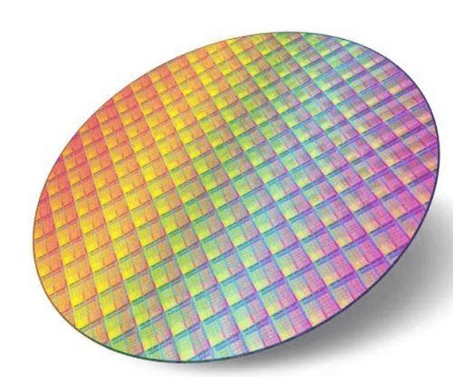
No industry is more sensitive to material purity than semiconductor manufacturing. Fabricating transistors with 7nm or even 5nm nodes leaves zero room for chemical variability. From barrier layers to gate oxides and interconnects, every thin film must be atomically precise and contamination-free. High purity sputtering targets ensure each deposited layer adheres to strict uniformity, preventing defects during etching and lithography.
Photovoltaics and Solar Energy
Modern thin-film solar cells, particularly CdTe and CIGS technologies, depend on the chemical integrity of absorber layers. The presence of impurities in targets like cadmium, selenium, and tellurium can lower conversion efficiency and increase degradation under UV exposure. This is especially crucial as the solar industry pushes toward lower cost-per-watt benchmarks.
Displays and Touch Panels
Advanced display technologies—from OLED to QLED—require high-performance transparent electrodes and buffer layers. Uniformity in ITO and ZnO films directly impacts brightness, touch sensitivity, and device longevity. With consumer expectations constantly rising, the margin for error is effectively zero.
Medical and Aerospace Applications
Medical imaging devices and aerospace sensors rely on ultra-pure films for accuracy and reliability under stress. Contaminants in thin films used for X-ray sensors or satellite coatings can cause failure under radiation or thermal cycling.
🔥 Top 10 FAQs
- Why is 99.999% purity important in sputtering targets?
High-purity sputtering targets minimize contamination in thin film deposition, ensuring better electrical, optical, and structural performance in applications like semiconductors and photovoltaics. - How do impurities affect thin film quality?
Even trace impurities can cause film defects, reduced adhesion, electrical failures, or optical distortion, especially in sensitive applications like microelectronics and optical coatings. - What materials are commonly used for high purity sputtering targets?
Common high-purity target materials include copper (Cu), aluminum (Al), molybdenum (Mo), tantalum (Ta), indium tin oxide (ITO), and titanium (Ti). - How is thin film deposition impacted by the target’s purity?
Higher purity leads to more uniform films with fewer defects, lower particle contamination, and better reproducibility, critical in processes like magnetron sputtering and PVD. - Which industries require 99.999% pure sputtering targets?
Industries include semiconductor manufacturing, solar energy, displays (OLED/QLED), data storage, medical imaging, and aerospace electronics. - How can I verify the purity of a sputtering target?
Techniques like GDMS (Glow Discharge Mass Spectrometry) and ICP-MS (Inductively Coupled Plasma Mass Spectrometry) are used to certify material purity. - What is the difference between 99.9%, 99.99%, and 99.999% target materials?
Each additional “9” reduces impurity levels by an order of magnitude. 99.999% (5N) purity offers dramatically lower contaminant levels, essential for precision thin films. - Does higher purity always improve thin film performance?
In most advanced applications, yes. High purity ensures consistent deposition and minimal performance degradation, especially for devices operating at nanoscale dimensions. - Who is a reliable sputtering target supplier for high-purity materials?
Leading suppliers like TFM (Thin Film Materials) specialize in producing 5N purity targets for critical industries including semiconductors and optical electronics. - Is high-purity material worth the higher cost?
Absolutely. While 5N targets are more expensive, they reduce failure rates, increase device reliability, and lower long-term production costs by improving yields.
Conclusion: Purity Is Precision, Precision Is Power
In the realm of advanced materials science, purity is not a luxury—it’s a necessity. A 99.999% pure sputtering target isn’t just a number on a spec sheet; it’s a reflection of the manufacturer’s commitment to performance, reliability, and innovation.
As thin film deposition techniques continue to scale into atomic dimensions, and as industries demand ever more from materials, the choice of high purity sputtering targets will be the silent force driving the future. From improved yield in semiconductor fabrication to enhanced transparency in optical coatings, the investment in ultra-pure materials pays dividends in performance.
If you’re an engineer, researcher, or sourcing manager aiming for excellence, never settle for less than five nines. The future of your device may very well depend on it.