Introduction
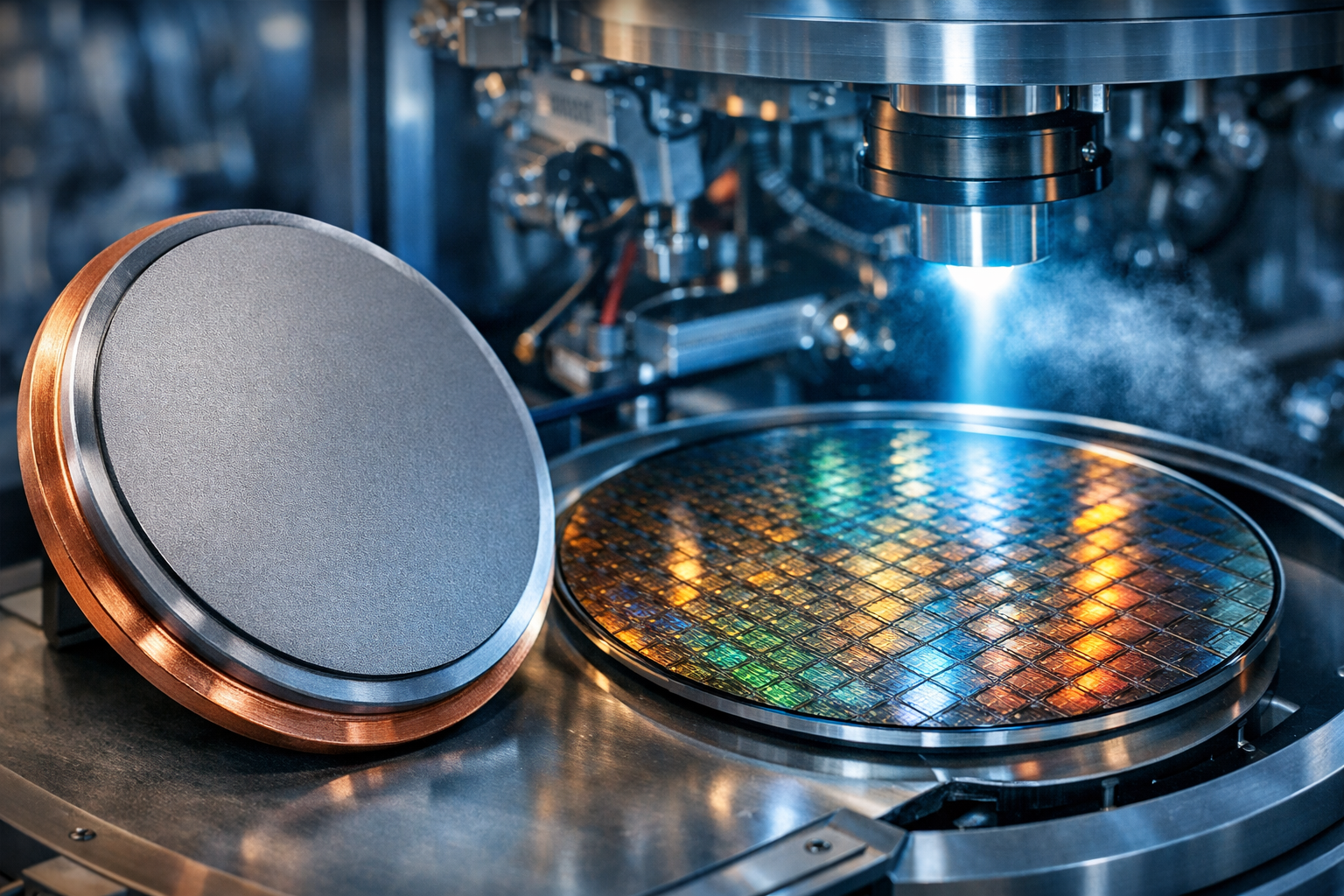
As semiconductor devices continue to scale toward advanced nodes such as 7 nm, 5 nm, and beyond, the demand for high-performance thin film materials has become increasingly critical. Among these materials, Tantalum (Ta) sputtering targets play a vital role in forming barrier layers that ensure device reliability, electrical integrity, and long-term stability.
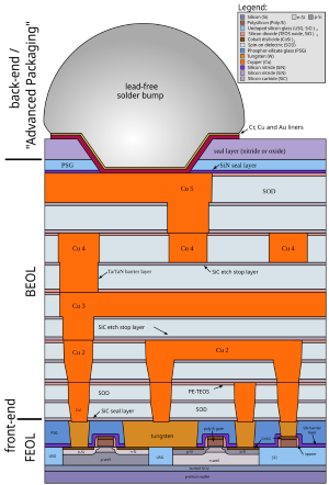
Barrier layers are essential in preventing diffusion between different materials—particularly copper interconnects and surrounding dielectric layers—where even atomic-scale diffusion can degrade performance or lead to device failure. Tantalum, with its unique combination of high density, excellent chemical stability, and superior diffusion resistance, has become a preferred material in advanced semiconductor fabrication.
What Are Semiconductor Barrier Layers?
Barrier layers are ultra-thin films deposited between conductive and insulating layers within semiconductor devices. Their primary function is to prevent interdiffusion and chemical reactions that can compromise electrical performance.
In modern integrated circuits, copper is widely used as the interconnect material due to its low resistivity. However, copper atoms can easily diffuse into surrounding dielectric materials, causing leakage currents and reliability issues. To address this, a barrier layer—typically made of materials like tantalum or tantalum nitride (TaN)—is deposited to act as a protective interface.
Why Tantalum Is Ideal for Barrier Layer Applications
1. Exceptional Diffusion Barrier Properties
Tantalum exhibits extremely low diffusivity for copper atoms, making it highly effective in preventing copper migration. This property is crucial for maintaining the integrity of interconnect structures, especially as device dimensions shrink.
2. High Thermal Stability
Semiconductor manufacturing processes often involve high temperatures. Tantalum maintains structural stability and does not degrade under thermal cycling, ensuring consistent performance during fabrication and operation.
3. Strong Adhesion to Substrates
Tantalum films adhere well to a variety of substrates, including silicon, silicon dioxide, and low-k dielectrics. This strong adhesion improves film durability and reduces the risk of delamination.
4. Excellent Corrosion Resistance
Tantalum is highly resistant to chemical corrosion, which is particularly important in harsh processing environments such as plasma etching and chemical vapor deposition (CVD).
5. Compatibility with Advanced Deposition Techniques
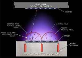
Tantalum sputtering targets are compatible with DC magnetron sputtering, RF sputtering, and advanced PVD systems, enabling precise control over film thickness and uniformity.
Tantalum vs Tantalum Nitride (Ta vs TaN)
In semiconductor barrier applications, both pure tantalum and tantalum nitride are widely used. Each material offers distinct advantages:
| Material | Key Characteristics | Typical Use |
|---|---|---|
| Tantalum (Ta) | High conductivity, excellent adhesion | Adhesion layer |
| Tantalum Nitride (TaN) | Superior diffusion barrier, higher resistivity | Barrier layer |
In many cases, a Ta/TaN bilayer structure is employed, where tantalum provides strong adhesion to the substrate while TaN acts as the primary diffusion barrier.
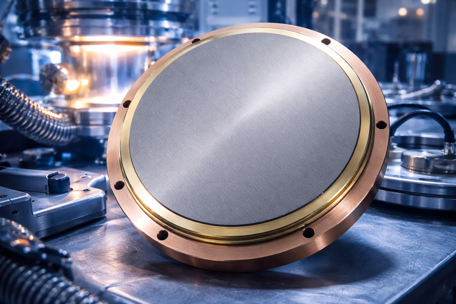
Manufacturing of Tantalum Sputtering Targets
The performance of a tantalum sputtering target directly influences the quality of the deposited thin film. High-quality targets are produced through advanced metallurgical processes:
Powder Metallurgy and Refining
High-purity tantalum powder is first refined to remove impurities. The powder is then compacted and sintered to achieve high density.
Hot Isostatic Pressing (HIP)
HIP is used to eliminate internal porosity and improve mechanical strength, resulting in a dense and uniform microstructure.
Precision Machining
The target is machined to precise dimensions, ensuring compatibility with sputtering systems and uniform erosion during deposition.
Bonding to Backing Plates
For large or high-power applications, tantalum targets are often bonded to copper or titanium backing plates to enhance heat dissipation and mechanical stability.
Key Performance Factors of Tantalum Targets
Purity
High purity (typically 99.95% to 99.99%) is essential to minimize contamination and ensure high-quality thin films.
Density
Targets with density greater than 95% of theoretical density provide better sputtering efficiency and film uniformity.
Grain Structure
Fine and uniform grain size contributes to consistent sputtering rates and reduces the risk of particle generation.
Bonding Quality
Reliable bonding between the target and backing plate is critical for thermal management and operational stability.
Applications in Advanced Semiconductor Devices
Tantalum sputtering targets are widely used in:
- Integrated Circuits (ICs) – Barrier layers for copper interconnects
- Logic Devices – Advanced node chips requiring ultra-thin diffusion barriers
- Memory Devices – DRAM and NAND flash technologies
- Power Electronics – High-reliability devices operating under harsh conditions
- AI and High-Performance Computing Chips – Demanding stable and reliable interconnect structures
Challenges and Future Trends
Scaling to Ultra-Thin Layers
As devices shrink, barrier layers must become thinner while maintaining effectiveness. This places higher demands on target purity and deposition control.
Advanced Materials Integration
New materials and structures, such as low-k dielectrics and 3D architectures, require improved barrier performance.
Sustainability and Cost Efficiency
Optimizing target utilization and reducing material waste are becoming increasingly important in semiconductor manufacturing.
FAQ
| Question | Answer |
|---|---|
| What purity is recommended for tantalum sputtering targets? | Typically 99.95% to 99.99% for semiconductor applications. |
| Can tantalum targets be customized? | Yes, dimensions, purity, and bonding options can be tailored. |
| What is the difference between Ta and TaN targets? | Ta is mainly used for adhesion, while TaN provides diffusion barrier properties. |
| What bonding options are available? | Indium bonding, elastomer bonding, and diffusion bonding are common. |
| Which deposition methods are compatible? | DC and RF magnetron sputtering are widely used. |
Conclusion
Tantalum sputtering targets are indispensable in modern semiconductor manufacturing, particularly in the formation of advanced barrier layers. Their superior diffusion resistance, thermal stability, and compatibility with cutting-edge deposition technologies make them a cornerstone material in the evolution of microelectronics.
As the industry moves toward increasingly complex device architectures and smaller feature sizes, the demand for high-performance tantalum targets will continue to grow. Selecting high-quality, customizable sputtering targets is essential for achieving optimal thin film performance and ensuring long-term device reliability.
For detailed specifications and a quotation, please contact us at sales@thinfilmmaterials.com.