The semiconductor industry is at the forefront of modern technology, underpinning innovations from consumer electronics to advanced computing systems. As devices continue to shrink in size while increasing in performance and complexity, the manufacturing techniques at the heart of semiconductor production must evolve accordingly. Sputtering—a physical vapor deposition (PVD)[1] method used to deposit thin films on substrates—has become an indispensable tool.This article explores the critical role that iridium sputtering targets play in semiconductor manufacturing, detailing their properties, production methods, applications, and future trends, all organized with clear hierarchical headings.
Introduction
Semiconductor manufacturing involves the precise layering of materials to create the complex structures found in integrated circuits. Among the many techniques used, sputtering stands out due to its ability to produce uniform, high-quality thin films. Within this context, sputtering targets made from noble metals like iridium have garnered significant interest. Owing to its exceptional physical and chemical properties, iridium is ideally suited for demanding applications where durability and stability are paramount. This article examines the technical and practical aspects of iridium sputtering targets and their indispensable contribution to semiconductor technology.
Overview of Semiconductor Manufacturing
Semiconductor devices serve as the building blocks of modern electronics, featuring in products ranging from smartphones to automotive control systems. The fabrication process includes several intricate steps:
- Photolithography: Patterning the wafer using light-sensitive materials.
- Etching: Removing material to create defined structures.
- Doping: Introducing impurities to modify electrical properties.
- Thin Film Deposition: Laying down ultra-thin layers to form conductive, insulating, or active regions.
Thin film deposition is particularly critical because the integrity, uniformity, and adhesion of these layers directly influence device performance. Sputtering is a favored deposition technique because it ensures high purity, excellent adhesion, and precise control over film thickness—qualities essential for the next generation of semiconductor devices.
Fundamentals of Sputtering Technology
Sputtering is a process where atoms are ejected from a solid target material due to bombardment by energetic particles, typically ions from a plasma. These liberated atoms travel through a vacuum and eventually deposit onto a substrate, forming a thin film. There are several sputtering methods, each tailored for specific applications.
Sputtering Techniques
Direct Current (DC) Sputtering
- Application: Primarily used for conductive targets.
- Mechanism: A steady electric field generates the plasma required for sputtering.
- Advantages: Simplicity and stability for conductive materials.
Radio Frequency (RF) Sputtering
- Application: Suitable for both conductive and insulating targets.
- Mechanism: Uses an alternating electric field to maintain the plasma.
- Advantages: Versatility in processing a wide range of materials.
Magnetron Sputtering
- Application: Enhances the sputtering process for various materials.
- Mechanism: Magnetic fields trap electrons near the target surface, increasing ionization rates and deposition efficiency.
- Advantages: Higher deposition rates and improved film quality.
Each of these techniques offers distinct benefits, with process parameters such as power, pressure, and substrate temperature carefully controlled to achieve the desired film properties. The versatility of sputtering in coating large areas with excellent uniformity and high purity makes it a preferred choice in semiconductor fabrication.
Iridium: A Noble Metal with Exceptional Properties

Iridium is one of the rarest and most corrosion-resistant metals on the periodic table, and its unique attributes make it particularly valuable in high-performance applications. Its key properties include:
High Melting Point
- Benefit: Iridium’s high melting point ensures stability during high-temperature processing steps in semiconductor fabrication.
- Impact: Maintains film integrity and prevents degradation during thermal cycles.
Chemical Inertness
- Benefit: Exceptional resistance to oxidation and corrosion.
- Impact: Ensures that deposited films remain stable and free from contamination over time.
Electrical Conductivity
- Benefit: Provides reliable conductivity, crucial for electrical contacts and interconnects.
- Impact: Balances performance with durability, even though it is not as conductive as some other metals like copper.
Mechanical Strength
- Benefit: Iridium’s hardness and robust structure contribute to its longevity.
- Impact: Reduces wear during prolonged sputtering operations and maintains consistent deposition rates.
These properties not only make iridium an ideal material for sputtering targets but also enhance the performance of the thin films it produces, thereby contributing to the reliability and efficiency of semiconductor devices.
The Role of Iridium Sputtering Targets in Semiconductor Manufacturing
Iridium sputtering targets are integral to several critical functions within semiconductor manufacturing. Their unique properties translate into practical applications that ensure device performance and longevity.
Thin Film Deposition for Contacts and Interconnects
- Function: Used in forming electrical contacts and interconnects.
- Benefit: High thermal stability and chemical inertness ensure that these conductive pathways remain reliable even under extreme conditions.
Barrier Layers
- Function: Act as barriers to prevent unwanted diffusion of metals into semiconductor substrates.
- Benefit: Iridium’s resistance to diffusion helps maintain device performance and extends operational life.
Electrode Fabrication
- Function: Employed in the creation of electrodes for specialized applications such as microelectromechanical systems (MEMS) and sensors.
- Benefit: Provides durability and stable electrical performance under harsh environmental conditions.
Catalytic Layers
- Function: Used to deposit catalytic layers that facilitate specific chemical reactions during manufacturing.
- Benefit: Enhances efficiency and selectivity, leading to improved overall device performance.
Optical Applications
- Function: Applied in optical coatings and reflective layers in photonic devices.
- Benefit: Offers precise control over film thickness and refractive index, critical for optical performance.
The multifunctionality of iridium sputtering targets underscores their significance in modern semiconductor fabrication processes, where each layer contributes to the overall performance and reliability of the final device.
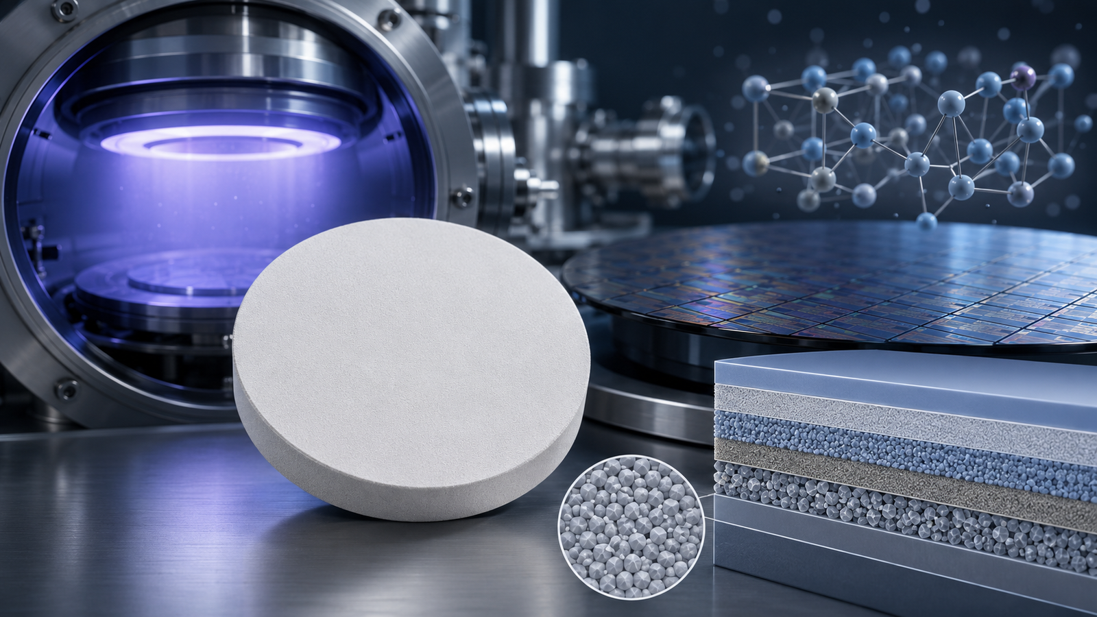
Production and Fabrication of Iridium Sputtering Targets
The production of high-quality iridium sputtering targets is a complex, multi-step process that emphasizes purity, precision, and durability.
Material Purification
- Process: The raw iridium is subjected to rigorous purification processes to eliminate impurities.
- Importance: High-purity iridium is essential to prevent defects in the deposited films, which could compromise device performance.
Melting and Alloying
- Process: Iridium is melted and sometimes alloyed with other metals to optimize its properties for sputtering.
- Importance: Alloying helps balance thermal stability, hardness, and sputtering yield, tailoring the target to specific manufacturing needs.
Forming and Machining
- Process: The purified or alloyed iridium is cast into the desired shapes and then precisely machined.
- Importance: Uniform thickness and a smooth surface are critical for achieving consistent sputtering rates and high-quality film deposition.
Surface Treatments
- Process: Post-machining, the target surface may be polished or treated with adhesion layers.
- Importance: Enhances target longevity and improves film uniformity by minimizing surface imperfections.
Quality Control
- Process: Throughout production, rigorous testing—including scanning electron microscopy (SEM) and energy-dispersive X-ray spectroscopy (EDX)—ensures the target meets stringent specifications.
- Importance: Maintaining high quality in every step is essential to ensure the reliability and performance of the sputtering target during semiconductor manufacturing.
Each step in the fabrication process is critical, as any deviation can affect the final product’s performance and, by extension, the quality of the semiconductor devices produced.
Advantages of Using Iridium Sputtering Targets
The use of iridium sputtering targets in semiconductor manufacturing offers several distinct advantages:
Enhanced Thermal Stability
- Explanation: The high melting point of iridium ensures that the target remains stable during high-temperature sputtering processes.
- Benefit: Leads to more reliable and consistent deposition processes.
Improved Film Quality
- Explanation: Iridium’s chemical inertness minimizes the risk of contamination during deposition.
- Benefit: Produces thin films that are pure, uniform, and free from defects.
Durability and Longevity
- Explanation: The robust mechanical properties of iridium contribute to a longer operational lifespan.
- Benefit: Reduces the frequency of target replacement, lowering production costs over time.
Compatibility with High-Performance Applications
- Explanation: The unique combination of iridium’s physical properties makes it suitable for use in environments requiring high durability.
- Benefit: Ensures that semiconductor devices perform reliably under extreme conditions such as high temperatures and corrosive atmospheres.
Precision in Film Thickness and Composition
- Explanation: Consistent sputtering rates facilitate precise control over the deposited film’s thickness.
- Benefit: Critical for the production of miniaturized and complex semiconductor devices.
These advantages explain why iridium sputtering targets are increasingly preferred in advanced semiconductor manufacturing, contributing to higher performance and longer-lasting devices.
Challenges in the Use of Iridium Sputtering Targets
Despite their many benefits, iridium sputtering targets also present several challenges that manufacturers must address.
High Material Cost
- Challenge: Iridium is one of the rarest and most expensive metals.
- Impact: The high cost of iridium can drive up the overall expenses in semiconductor manufacturing, necessitating a balance between performance benefits and economic considerations.
Complex Fabrication Process
- Challenge: The production of high-purity iridium targets requires sophisticated techniques and stringent quality control.
- Impact: Any deviation during fabrication can lead to performance issues in the final product, making precision and consistency paramount.
Sputtering Efficiency
- Challenge: Achieving a high sputtering yield with iridium can be more difficult compared to other materials.
- Impact: Optimizing process parameters is essential to ensure efficient material utilization and maintain high deposition rates.
Equipment Compatibility
- Challenge: Integrating iridium sputtering targets into existing sputtering systems may require modifications.
- Impact: Adjustments in power settings, substrate bias, or vacuum conditions might be necessary to accommodate the unique characteristics of iridium, adding complexity to the manufacturing process.
Addressing these challenges is crucial for maximizing the benefits of iridium sputtering targets while maintaining cost-effectiveness in semiconductor manufacturing.
Advances in Iridium Sputtering Target Technology
Continuous research and development are driving improvements in the performance and reliability of iridium sputtering targets. Key areas of innovation include:
Target Composition and Alloying
- Innovation: Researchers are developing new alloy compositions that blend iridium with other elements.
- Objective: Enhance sputtering efficiency, reduce costs, and improve film properties while retaining iridium’s desirable attributes.
Optimized Deposition Techniques
- Innovation: Advanced techniques such as high-power impulse magnetron sputtering (HiPIMS) offer improved ionization and energy control.
- Objective: Achieve better film quality and maximize the performance of iridium sputtering targets under challenging processing conditions.
Surface Engineering
- Innovation: Methods such as laser surface modification and advanced polishing techniques are being applied.
- Objective: Reduce surface roughness, thereby improving the uniformity of the sputtered films and extending the target’s life.
Modeling and Simulation
- Innovation: Advanced computational models simulate the sputtering process to better understand ion-target interactions.
- Objective: Guide the development of targets with optimized microstructures and improved sputtering behaviors.
Sustainability Considerations
- Innovation: Efforts are underway to extend target lifetimes and improve material utilization.
- Objective: Enhance the sustainability of semiconductor manufacturing by reducing waste and recycling expensive materials like iridium.
These technological advances not only improve the performance of iridium sputtering targets but also pave the way for their use in next-generation semiconductor devices.
Impact on Semiconductor Device Performance
The quality and characteristics of thin films deposited using iridium sputtering targets have a direct impact on the performance and reliability of semiconductor devices. Key performance aspects include:
Electrical Performance
- Contribution: High-quality iridium films provide stable electrical pathways with low resistivity.
- Outcome: Essential for high-speed microprocessors, memory devices, and other integrated circuits where electrical performance is critical.
Reliability and Durability
- Contribution: The use of iridium helps mitigate issues such as electromigration and metal diffusion.
- Outcome: Enhances the long-term reliability and operational lifespan of semiconductor devices, even under extreme conditions.
Miniaturization and Precision
- Contribution: Consistent sputtering rates enable the deposition of ultra-thin films with tight control over thickness and composition.
- Outcome: Supports ongoing trends in device miniaturization and the fabrication of increasingly complex circuit architectures.
Performance in Harsh Environments
- Contribution: Devices that incorporate iridium-based layers exhibit superior performance under high temperature, corrosive, or mechanically stressful conditions.
- Outcome: Expands the range of applications for semiconductor devices, including automotive, aerospace, and industrial control systems.
The integration of iridium sputtering targets into semiconductor fabrication processes is instrumental in achieving the performance metrics required by today’s advanced electronic devices.
Future Trends and Outlook
As the semiconductor industry continues to push the boundaries of performance and miniaturization, the role of advanced materials like iridium in sputtering targets is expected to grow. Emerging trends and developments include:
Integration with Next-Generation Devices
- Trend: New device architectures such as quantum computing, flexible electronics, and advanced sensors require materials with high performance and durability.
- Outlook: Iridium’s unique properties position it as a key enabler for these emerging technologies.
Process Optimization and Automation
- Trend: Advances in process control, real-time monitoring, and automation are streamlining the use of sputtering targets.
- Outlook: Improved diagnostics and control mechanisms will enhance target utilization and reduce manufacturing costs.
Cross-Disciplinary Applications
- Trend: Beyond traditional semiconductor applications, innovations in fields like renewable energy and biotechnology may benefit from iridium-based thin films.
- Outlook: The broader adoption of iridium sputtering targets could drive further research into new target materials and deposition techniques.
Sustainable Manufacturing
- Trend: There is an increasing focus on sustainability and resource efficiency within the semiconductor industry.
- Outlook: Techniques that extend target lifetimes and improve material utilization will contribute to more sustainable manufacturing practices, reducing waste and lowering overall costs.
Academic and Industry Collaboration
- Trend: Partnerships between research institutions and semiconductor manufacturers are fostering innovation.
- Outlook: Such collaborations are expected to yield new insights into sputtering processes and lead to further enhancements in target technology.
These trends underscore the ongoing evolution of sputtering target technology and affirm iridium’s role as a critical material in the advancement of semiconductor devices.
Conclusion
Iridium sputtering targets represent a significant advancement in semiconductor manufacturing. Their unique combination of thermal stability, chemical inertness, and mechanical strength makes them an invaluable component in the deposition of ultra-thin films that are essential for modern electronic devices. From the formation of reliable electrical contacts and barrier layers to supporting the miniaturization of devices and enhancing performance in harsh environments, iridium sputtering targets have a profound impact on semiconductor device performance.
The journey from raw iridium to a high-performance sputtering target exemplifies the sophistication of modern materials engineering. As the semiconductor industry faces ever-growing demands for higher performance and greater reliability, the development and refinement of sputtering target technology remain critical. Continuous improvements in target fabrication, deposition techniques, and process optimization promise to deliver even greater efficiencies and breakthroughs in device performance.
Looking ahead, the integration of iridium sputtering targets with next-generation device architectures, coupled with advancements in automation and sustainability, will ensure that these materials remain at the forefront of semiconductor manufacturing. The collaboration between academia and industry will further drive innovation, overcoming challenges and opening up new avenues for application.
In essence, the evolution of iridium sputtering target technology is a testament to the relentless pursuit of excellence in semiconductor fabrication. As the industry continues to innovate, the role of iridium in shaping the future of electronics becomes ever more critical, proving that even the thinnest of films can make the biggest impact.
This comprehensive exploration highlights the transformative role of iridium sputtering targets in semiconductor manufacturing—a field where precision, reliability, and innovation converge to power the technology of tomorrow.