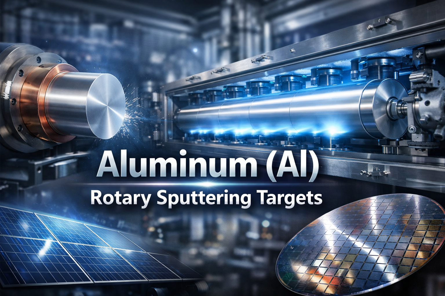
Introduction
Thin film technology has become a cornerstone of modern industrial advancement, powering innovations in semiconductors, aerospace, energy systems, and medical devices. At the heart of these applications lies the critical process of sputtering, a physical vapor deposition (PVD) method that deposits extremely thin layers of material onto substrates. While the sputtering technique is versatile, the choice of sputtering material significantly impacts the quality, efficiency, and durability of the resulting films—especially under extreme conditions.
Among the numerous sputtering materials available, tantalum (Ta) has earned a stellar reputation for high-temperature applications. Thanks to its extraordinarily high melting point, resistance to chemical attack, strong mechanical integrity, and impressive thermal and electrical properties, tantalum is widely used where performance and reliability are paramount. In this article, we explore why tantalum is ideally suited for high-temperature sputtering, comparing its characteristics with alternative materials, examining its industrial uses, and uncovering the science that makes it indispensable in demanding applications.
The Fundamentals of High-Temperature Sputtering
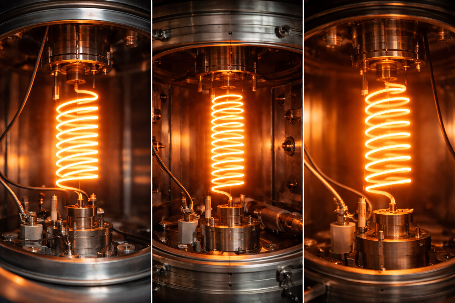
Sputtering involves the bombardment of a solid target material with high-energy ions (usually argon plasma), causing atoms to be ejected from the target and deposited as a thin film onto a substrate. This technique allows for precision control over thickness, composition, and film morphology, making it essential in applications ranging from electronics to optics.
However, not all sputtering environments are created equal. In many advanced manufacturing sectors, sputtering occurs at elevated temperatures, either due to:
- Intentional substrate heating (to enhance adhesion or crystallinity),
- High plasma power settings,
- Long deposition durations,
- Or the use of reactive gases (e.g., oxygen or nitrogen) that generate thermal stress.
In such conditions, target materials must maintain structural integrity, resist thermal degradation, and ensure compositional purity throughout the process. Tantalum rises above most alternatives in these areas.
Key Physical Properties of Tantalum for High-Temperature Performance
Extreme Melting Point
Tantalum’s most notable physical trait is its melting point of 3017°C (5463°F)—one of the highest among all elements. This property makes it exceptionally suited for:
- Thermal stability under prolonged high-power sputtering.
- Compatibility with high-temperature substrates like sapphire or quartz.
- Avoiding deformation or vaporization during deposition.
Materials like titanium (melting point: 1668°C) and aluminum (660°C) cannot match this resilience, making tantalum a natural choice for high-temperature sputtering systems.
Thermal Conductivity and Expansion
Tantalum has a thermal conductivity of approximately 57 W/m·K, which is moderate but sufficient to evenly distribute heat across the target. More importantly, it has a low coefficient of thermal expansion (~6.3 µm/m·K), which minimizes the risk of thermal stress and warping during heating and cooling cycles. These factors make tantalum targets more resistant to cracking and ensure dimensional stability, which is crucial for applications demanding uniform film thickness and consistency.
Mechanical Strength and Workability
At room temperature and elevated temperatures, tantalum maintains a balance between hardness, ductility, and toughness:
- Tensile strength at room temp: ~200 MPa.
- Hardness: 60–120 HB.
- High modulus of elasticity: ~186 GPa.
These mechanical attributes reduce the chances of target damage during handling, bonding, or prolonged operation. Moreover, tantalum can be easily fabricated into custom shapes (discs, rectangular slabs, ring targets) and bonded to various backing plates, supporting widespread industrial use.
Superior Chemical Stability in Harsh Environments
Oxidation and Corrosion Resistance
Tantalum is chemically inert to most acids and reactive gases. It forms a dense, adherent oxide film (Ta₂O₅) upon exposure to oxygen, which protects the underlying metal from further oxidation or attack. This is especially beneficial during reactive sputtering, where gases like oxygen or nitrogen are introduced to produce oxide or nitride films. Where other metals suffer degradation or contamination, tantalum remains:
- Stable,
- Durable,
- And clean in its deposition behavior.
Compatibility with Reactive and Harsh Gases
In high-temperature sputtering, oxygen, nitrogen, and even fluorine can attack conventional metals. Tantalum, however, is used in:
- Reactive sputtering to produce TaN or Ta₂O₅ thin films,
- Plasma-enhanced processes without breakdown or contamination,
- Corrosive vacuum environments where materials like copper, silver, or chromium would fail.
These properties make tantalum highly desirable for sputtering in vacuum chambers, gloveboxes, and ultra-high vacuum (UHV) systems.
Electronic and Magnetic Behavior in Sputtering
Electrical Conductivity
Tantalum has an electrical resistivity of 13.5 µΩ·cm, positioning it between highly conductive metals like copper and less conductive ceramics. This moderate conductivity allows:
- Efficient power transfer during DC sputtering,
- Stable plasma generation in RF systems,
- Excellent performance in electronic thin film components such as:
- Capacitor electrodes,
- Gate electrodes,
- Interconnect barriers.
In capacitor production, tantalum films often serve as a base for growing tantalum pentoxide, a high-k dielectric that enables high capacitance in a small volume.
Non-Magnetic Nature
Tantalum is paramagnetic, meaning it exhibits no permanent magnetic field. This is critical in:
- Magnetron sputtering systems, where magnetic fields control plasma density.
- Thin-film heads in hard drives or sensors, where magnetic interference must be minimized.
- High-frequency applications, where eddy currents and field interactions must be reduced.
Compared to ferromagnetic materials like nickel or iron, tantalum allows for a clean, interference-free sputtering process, particularly useful in integrated circuits and MEMS devices.
Industrial Applications of Tantalum Thin Films
1. Semiconductors
Tantalum is a staple in the semiconductor industry for its role in:
- Barrier layers in copper interconnects (preventing Cu diffusion),
- High-k dielectric films for DRAM and flash memory,
- Gate metal in CMOS transistors,
- Electromigration-resistant coatings.
As devices shrink, the thermal and chemical stability of materials becomes paramount—areas where tantalum consistently delivers.
2. Aerospace and Energy
Tantalum sputtered films are used in:
- High-temperature coatings on turbine components,
- Solar absorbers in space applications,
- Encapsulation of high-power electronics exposed to extreme conditions.
Its ability to withstand thermal cycling, radiation, and oxidation makes it ideal for space, military, and nuclear technology sectors.
3. Medical Devices
Due to its biocompatibility, tantalum is used for thin film coatings on:
- Implantable electronic devices (e.g., pacemakers),
- Medical sensors,
- Orthopedic tools requiring anti-corrosion properties.
Thin tantalum layers can also improve adhesion, reduce inflammation risk, and support better integration with tissue in biomedical devices.
4. Optics and Photonics
Tantalum pentoxide (Ta₂O₅), a derivative of tantalum sputtering, is a high-index optical material used in:
- Anti-reflection coatings,
- Laser mirrors,
- Photonic integrated circuits.
It offers broadband transmission, low optical loss, and excellent environmental durability.
Tantalum Target Preparation and Bonding for Sputtering
Target Shapes and Customization
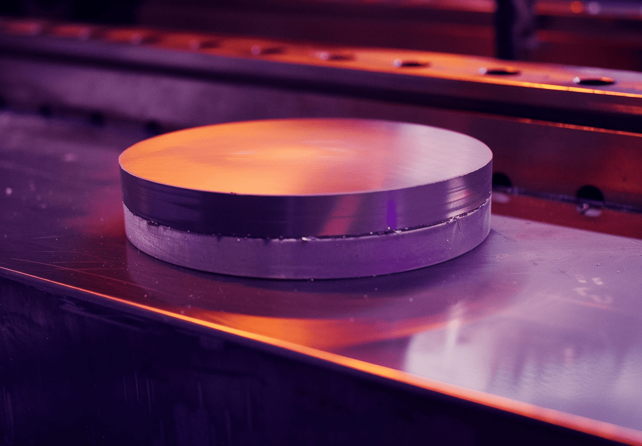
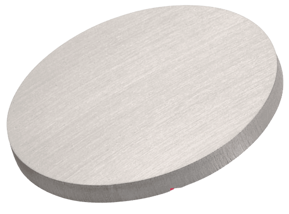
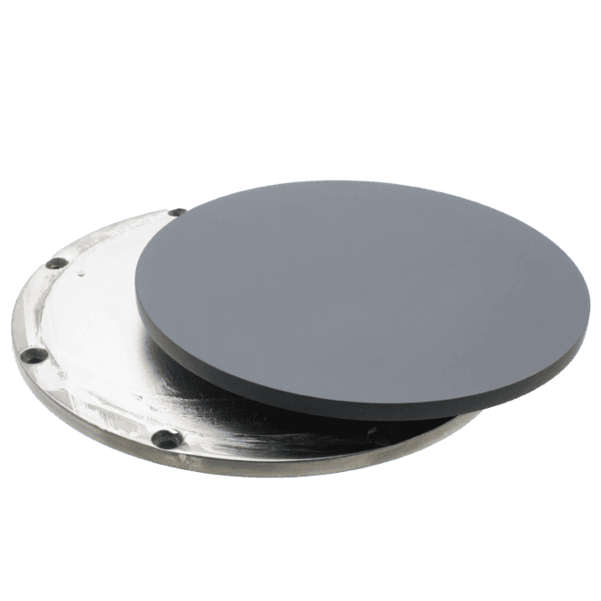
At TFM, tantalum targets are manufactured to custom specifications:
- Disc targets for circular sputter sources.
- Rectangular targets for inline coaters.
- Ring-shaped targets for large-area sputtering.
- Available in high purity levels up to 99.999%.
Bonding Techniques
Due to tantalum’s density and thermal conductivity, it is often bonded to a copper or molybdenum backing plate using:
- Indium bonding (soft, thermally conductive),
- Elastomeric bonding (shock absorbent, chemically resistant),
- Solder bonding (durable for medium-high temperatures).
Proper bonding ensures:
- Improved heat dissipation,
- Reduced risk of cracking or delamination,
- Better lifespan and target utilization.
Learn more about bonding options at TFM’s target bonding service page.
Tantalum vs Other Sputtering Materials
| Material | Melting Point (°C) | Chemical Stability | Electrical Conductivity | Reactive Sputtering Suitability |
|---|---|---|---|---|
| Tantalum | 3017 | Excellent | High | Excellent |
| Molybdenum | 2623 | Good | Medium | Moderate |
| Tungsten | 3422 | Moderate | Medium | Low |
| Titanium | 1668 | Poor (oxidizes easily) | Low | High (but unstable) |
| Aluminum | 660 | Low | Very High | Low |
Tantalum stands out as the best compromise between chemical durability, sputter efficiency, and thin film performance.
Frequently Asked Questions (FAQs)
Q1: What forms of tantalum are used for sputtering?
Most sputtering targets use pure tantalum or occasionally tantalum alloys (e.g., Ta-W) depending on application needs. Tantalum oxide (Ta₂O₅) may also be used as a ceramic target.
Q2: Can tantalum be sputtered in reactive gas environments?
Yes. Tantalum works excellently in oxygen, nitrogen, or fluorine atmospheres to form functional thin films like TaN or Ta₂O₅.
Q3: What industries benefit most from tantalum sputtering?
Semiconductors, aerospace, optical coatings, energy systems, and medical electronics.
Q4: Does tantalum have any health or environmental hazards?
Tantalum is considered safe and non-toxic. It is also RoHS-compliant when used in electronics.
Q5: How long does a bonded tantalum target last?
Target life depends on power settings and coating area, but properly bonded targets from TFM can operate for hundreds of hours in production environments.
Conclusion
In the demanding realm of high-temperature thin film deposition, tantalum offers an unrivaled blend of thermal, mechanical, chemical, and electrical properties that make it ideal for sputtering applications. Whether used in the production of advanced semiconductors, aerospace coatings, medical devices, or high-index optical films, tantalum consistently delivers performance, purity, and durability where it matters most.
Backed by high-quality manufacturing, customizable formats, and robust bonding services, tantalum sputtering targets from TFM stand as the gold standard for engineers and researchers seeking uncompromising results in extreme environments.