Introduction: Why Niobium Silicide Matters in Modern Thin-Film Technology
As semiconductor devices, functional coatings, and precision electronic components continue to evolve toward higher integration, smaller dimensions, and harsher operating environments, material selection at the thin-film level has become increasingly critical. Traditional elemental metals often struggle to meet modern requirements for thermal stability, interfacial compatibility, and long-term reliability. This has driven growing interest in compound materials, particularly metal silicides, which bridge the gap between metals and semiconductors.
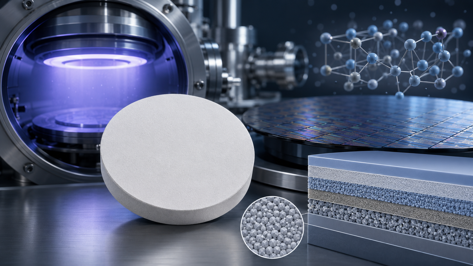
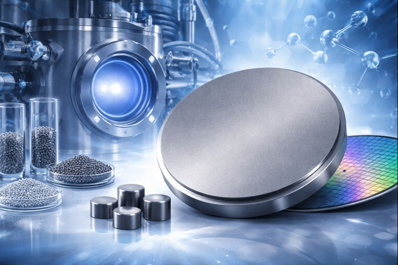
Among these materials, Niobium Silicide (NbSi₂) has emerged as a technically mature and industrially relevant option. When supplied in the form of a Niobium Silicide Sputtering Target, NbSi₂ enables direct deposition of uniform silicide films with controlled stoichiometry, stable electrical properties, and excellent thermal endurance. These characteristics make NbSi₂ especially attractive for semiconductor manufacturing, thin-film resistors, MEMS devices, and high-temperature functional coatings.
This article provides a detailed, application-oriented overview of NbSi₂ sputtering targets, focusing on their material properties, thin-film behavior, deposition advantages, and real-world use scenarios across advanced industries.
Understanding Niobium Silicide (NbSi₂) as a Material System
Composition and Crystal Structure
Niobium Silicide is an intermetallic compound formed between niobium (Nb) and silicon (Si), with NbSi₂ being the most widely used stoichiometric phase in thin-film applications. Unlike solid-solution alloys, NbSi₂ has a well-defined crystal structure, which contributes to its predictable physical and chemical behavior.
This ordered structure provides:
Stable phase formation during sputtering
Reduced compositional drift during target erosion
Consistent film properties across large substrates
From a thin-film engineering perspective, these attributes are essential for repeatability in both R&D and volume production.
Key Physical and Chemical Properties
NbSi₂ combines favorable properties from both constituent elements:
- High melting point (~1930 °C), supporting high-temperature processing
- Moderate and stable electrical conductivity, suitable for resistive and conductive films
- Excellent thermal stability, particularly under vacuum and inert atmospheres
- Good oxidation resistance compared with pure niobium films
- Strong compatibility with silicon substrates, minimizing interfacial stress
These properties position NbSi₂ between refractory metals and semiconductors, offering a balanced performance profile that is difficult to achieve with elemental materials alone.
Why Use a NbSi₂ Sputtering Target Instead of Elemental Targets?

Limitations of Co-Sputtering Nb and Si
In principle, niobium silicide films can be produced by co-sputtering separate Nb and Si targets. However, this approach introduces several challenges:
- Complex power balancing between targets
- Sensitivity to target aging and erosion rates
- Greater risk of stoichiometric deviation
- Reduced reproducibility between runs
In contrast, using a single NbSi₂ compound sputtering target simplifies process control and improves film uniformity.
Advantages of Direct Compound Target Sputtering
A NbSi₂ sputtering target allows:
- Direct deposition of silicide films without post-silicidation
- Stable composition across the target lifetime
- Simplified process recipes
- Lower risk of phase separation in deposited films
For industrial environments where yield, uptime, and consistency matter, these advantages often outweigh the higher initial material cost of compound targets.
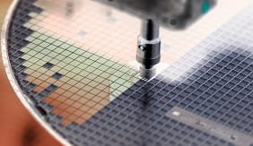
Thin-Film Deposition Behavior of NbSi₂
Sputtering Modes and Process Compatibility
NbSi₂ sputtering targets are compatible with common PVD systems, including:
- DC magnetron sputtering
- RF magnetron sputtering
- Pulsed DC sputtering
DC sputtering is typically preferred due to NbSi₂’s sufficient electrical conductivity, while RF sputtering may be used in systems optimized for compound materials or lower power densities.
Film Microstructure and Density
Deposited NbSi₂ films generally exhibit:
- Dense microstructures with low porosity
- Fine-grained or nanocrystalline phases
- Smooth surface morphology under optimized conditions
Film density and microstructure can be tuned through:
- Sputtering power
- Working gas pressure
- Substrate temperature
- Post-deposition annealing
These tunable parameters allow NbSi₂ films to be optimized for electrical, thermal, or mechanical performance depending on the application.
Core Application Scenarios for NbSi₂ Sputtering Targets
1. Semiconductor Manufacturing
Gate and Electrode Materials
In advanced semiconductor devices, NbSi₂ thin films are used as:
- Gate electrodes
- Contact layers
- Interfacial layers between silicon and metals
Compared with pure metals, NbSi₂ offers improved resistance to diffusion and agglomeration during high-temperature annealing, which is essential for maintaining device integrity during fabrication.
Backend-of-Line (BEOL) Compatibility
NbSi₂ films can withstand thermal budgets common in BEOL processes, reducing risks associated with:
- Film cracking
- Interdiffusion
- Electrical drift
This makes NbSi₂ particularly suitable for logic devices, power electronics, and specialized integrated circuits.
2. Thin-Film Resistors and Precision Electronics
NbSi₂ thin films exhibit stable resistivity over wide temperature ranges, making them ideal for:
- Precision thin-film resistors
- Resistor networks in analog circuits
- Temperature-stable electronic components
By adjusting deposition conditions and film thickness, engineers can tailor the resistivity and temperature coefficient of resistance (TCR) to meet specific design requirements.
3. MEMS and Micro-Heater Devices
Micro-electromechanical systems (MEMS) often operate under repeated thermal cycling and localized heating. NbSi₂ films are used in:
Micro-heaters
Thermal sensors
Structural conductive layers
Their thermal stability and adhesion to silicon-based substrates make them reliable choices for long-term MEMS operation.
4. High-Temperature Functional and Protective Coatings
NbSi₂ is well known in bulk form for its high-temperature performance. In thin-film form, it serves as:
A protective layer against thermal degradation
A functional coating in harsh vacuum environments
A diffusion-resistant interlayer
These applications are common in aerospace electronics, high-temperature sensors, and experimental energy devices.
5. Research and Advanced Functional Films
In academic and industrial R&D, NbSi₂ sputtering targets are used to explore:
- Novel silicide-based electronic materials
- Multilayer thin-film stacks
- Stress-engineered coatings
The predictable behavior of NbSi₂ films makes them valuable reference materials in materials science research.
Comparison with Related Materials
| Material | Key Limitation | NbSi₂ Advantage |
|---|---|---|
| Pure Niobium | Diffuses into Si at high temperature | Improved thermal and interfacial stability |
| Silicon | Low conductivity | Controlled electrical performance |
| Molybdenum | High stress, mismatch | Better Si compatibility |
| Tungsten | Difficult processing | Lower stress, easier deposition |
| Other silicides | Complex formation steps | Direct deposition from target |
This comparison highlights why NbSi₂ occupies a practical middle ground for many thin-film applications.
Target Manufacturing Considerations
Density and Microstructural Uniformity
High-quality NbSi₂ sputtering targets are typically manufactured using advanced powder metallurgy techniques to achieve:
- High relative density (≥ 98% theoretical)
- Uniform grain distribution
- Low impurity content
These factors directly influence sputtering stability, arcing behavior, and film quality.
Mechanical Characteristics
As an intermetallic compound, NbSi₂ is more brittle than pure metals, which affects:
- Handling procedures
- Bonding choices
- Packaging requirements
Proper target design and backing plate selection are essential to ensure safe installation and long service life.
Typical Technical Parameters (Representative)
| Parameter | Typical Range | Importance |
|---|---|---|
| Purity | 99.9% – 99.99% | Minimizes film defects |
| Density | ≥ 98% theoretical | Stable sputtering behavior |
| Diameter | 25 – 300 mm | System compatibility |
| Thickness | 3 – 6 mm | Target lifetime |
| Bonding | Cu backing / elastomer / indium | Thermal management |
Actual specifications can be customized according to sputtering system design and application needs.
Packaging, Handling, and Storage
NbSi₂ sputtering targets are typically:
- Vacuum sealed
- Moisture protected
- Shock cushioned
These measures preserve surface cleanliness and prevent micro-cracking during transport. Due to the brittle nature of silicides, careful handling is recommended during unpacking and installation.
Future Outlook for NbSi₂ Thin-Film Applications
As semiconductor technologies move toward higher temperatures, higher power densities, and more demanding reliability standards, the role of metal silicides like NbSi₂ is expected to grow. Emerging areas such as power electronics, wide-bandgap devices, and advanced sensors continue to drive demand for materials that combine conductivity, thermal stability, and compatibility with silicon ecosystems.
NbSi₂ sputtering targets are well positioned to support these trends due to their mature processing characteristics and proven performance.
Conclusion
Niobium Silicide Sputtering Targets (NbSi₂) offer a robust and versatile solution for depositing thermally stable, electrically functional thin films across a wide range of advanced applications. From semiconductor devices and thin-film resistors to MEMS and high-temperature coatings, NbSi₂ provides a unique balance of properties that elemental materials often cannot achieve.
For engineers, researchers, and industrial users seeking process simplicity, reproducibility, and long-term reliability, NbSi₂ sputtering targets represent a technically sound and future-ready material choice.
For detailed specifications, customization options, and pricing information, please contact sales@thinfilmmaterials.com.