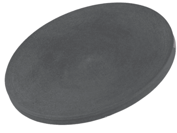
Niobium Nitride Sputtering Target Description
Niobium Nitride sputtering target from TFM is a nitride ceramic sputtering material with the chemical formula NbN. This material is known for its unique properties and applications in various high-performance industries, including electronics, superconductors, and optical coatings. Niobium Nitride sputtering targets are utilized in thin film deposition processes to create coatings that enhance the electrical, optical, and mechanical properties of surfaces.
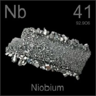
Niobium is a silver-colored metal typically found alongside tantalum. These two elements are often separated through fractional crystallization of their respective fluoro-complexes. Niobium has an abundance of approximately 20 parts per million (ppm) in the Earth’s crust. In its pure form, niobium is highly reactive, particularly when exposed to air, where it forms a stable oxide layer that significantly enhances its corrosion resistance. This metal also reacts with various non-metals at elevated temperatures, making it versatile for different industrial applications, including its use in superconducting materials, alloys, and specialized coatings.
Related Product: Niobium Sputtering Target
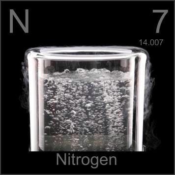 Nitrogen is a chemical element with the symbol “N” and atomic number 7. It derives its name from the Greek words ‘nitron’ and ‘genes,’ meaning nitre-forming. Nitrogen was first identified and isolated by Daniel Rutherford in 1772. It belongs to the p-block of the periodic table, situated in Period 2 and Group 15. The relative atomic mass of nitrogen is approximately 14.0067, with the number in brackets indicating the measurement’s uncertainty. Nitrogen is a fundamental component of the atmosphere, constituting around 78% of the Earth’s air by volume, and is essential for all known forms of life.
Niobium Nitride Sputtering Target Application
The niobium nitride (NbN) sputtering target is widely used in various applications, including thin film deposition for decoration, semiconductor devices, displays, LEDs, and photovoltaic devices. It is also utilized in creating functional coatings, which are essential in industries such as optical information storage, glass coating for automotive and architectural uses, and optical communication systems. This material’s properties make it valuable for enhancing the durability and functionality of coated surfaces across these diverse applications.
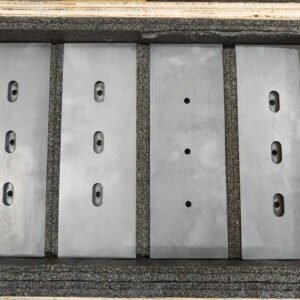
Niobium Nitride Sputtering Target Packaging
Our niobium nitride sputtering target is meticulously tagged and labeled externally for easy identification and stringent quality control. We take exceptional care in handling and packaging these targets to prevent any damage during storage or transportation, ensuring that the product arrives in pristine condition and maintains its quality throughout its use.
Get Contact
TFM offers Niobium Nitride Sputtering Targets in various forms, purities, sizes, and prices. We specialize in high-purity thin film deposition materials with optimal density and minimal grain sizes, which are ideal for semiconductor, CVD, and PVD applications in display and optics. Contact Us for current pricing on sputtering targets and other deposition materials that are not listed.


Reviews
There are no reviews yet.