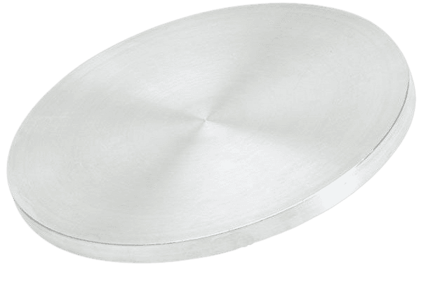
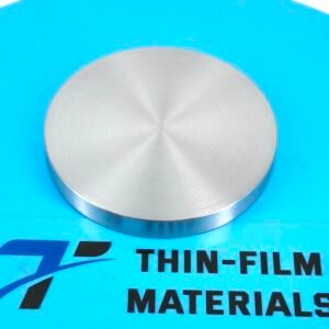
Aluminum Manganese Sputtering Target Description
Aluminum-Manganese sputtering targets are distinguished by their exceptional properties, which make them highly effective for thin film deposition applications. These targets are renowned for their excellent purity, ensuring reliable and consistent results in thin film preparation. They also offer strong electrical properties, making them particularly suitable for use in the semiconductor industry. The unique alloy combination imparts superior chemical stability, allowing these targets to maintain performance and stability throughout the thin film deposition process. These attributes make Aluminum-Manganese sputtering targets widely utilized across high-tech industries, supporting the advancement of cutting-edge technologies and various industrial applications.
Related Product: Manganese Sputtering Target, Manganese Oxide Sputtering Target
Aluminum Manganese Sputtering Target Specifications
| Compound Formula | Al/Mn |
| Appearance | Silver Metallic Target |
| Density | 2.72g/cm3 |
| Available Sizes | Dia.: 1.0″, 2.0″, 3.0″, 4.0″, 5.0″, 6.0″ Thick: 0.125″, 0.250″ |
Aluminum Manganese Sputtering Target Handling Notes
Indium bonding is recommended for Aluminum-Manganese sputtering targets due to their inherent characteristics, such as brittleness and low thermal conductivity, which can impact sputtering performance. The low thermal conductivity and susceptibility to thermal shock of this material make indium bonding a suitable choice to enhance its stability and effectiveness during the sputtering process.
Aluminum Manganese Sputtering Target Application
Aluminum Manganese Sputtering Target Packaging
Our Aluminum-Manganese sputtering targets are meticulously handled throughout storage and transportation to ensure they retain their quality and arrive in optimal condition.
Get Contact
TFM’s Aluminum-Manganese sputtering targets are offered in a variety of forms, purities, and sizes. We focus on producing high-purity physical vapor deposition (PVD) materials with maximum density and minimal average grain sizes. These targets are ideal for semiconductor applications, as well as for chemical vapor deposition (CVD) and PVD in display and optical technologies.


Reviews
There are no reviews yet.