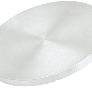
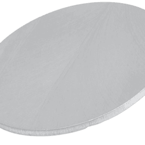
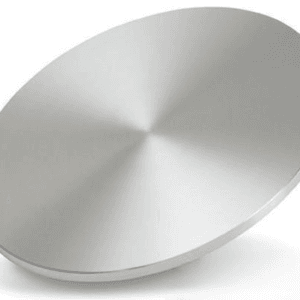
Antimony Indium Tin Sputtering Target
Introduction
The Antimony Indium Tin Sputtering Target is a multi-component alloy target designed for advanced thin film deposition. By combining the semiconducting properties of indium, the conductivity of tin, and the modifying characteristics of antimony, this material enables the production of films with tailored electrical, optical, and structural performance. It is particularly attractive for next-generation optoelectronic devices, transparent conductive coatings, and research in compound semiconductors.
Detailed Description
Antimony Indium Tin sputtering targets are manufactured through powder metallurgy and vacuum sintering, resulting in a dense, homogeneous target that delivers stable sputtering rates and uniform thin film composition.
Key features include:
High Purity (≥99.9%) – ensures low contamination and reproducible film properties.
Optimized Alloy Composition – Sb, In, and Sn can be tuned in different atomic ratios depending on customer requirements.
Stable Microstructure – minimizes cracking and enables long target life.
Custom Bonding Options – available with Indium or Elastomer bonding to copper backing plates for high-power sputtering systems.
These properties allow precise control of thin film characteristics, especially in applications where transparency, conductivity, and thermal stability must be balanced.
Applications
Antimony Indium Tin Sputtering Targets are widely used in:
Transparent Conductive Films (TCFs) – for displays, touch panels, and photovoltaics.
Semiconductor Devices – functional layers in electronic and optoelectronic components.
Thin Film Photovoltaics – coatings for solar cell electrodes and active layers.
Optical Coatings – films with tailored refractive and conductive properties.
R&D in Advanced Materials – studies on ternary/quaternary compound semiconductors.
Technical Parameters
| Parameter | Typical Value / Range | Importance |
|---|---|---|
| Purity | 99.9% – 99.99% | Ensures high-quality thin films |
| Composition | Sb/In/Sn (custom ratios available) | Tailors conductivity & transparency |
| Diameter | 25 – 200 mm | Fits standard sputtering systems |
| Thickness | 3 – 10 mm | Affects deposition stability |
| Bonding | Indium / Elastomer / Copper backing | Improves thermal management |
Comparison with Related Materials
| Material | Key Advantage | Typical Application |
|---|---|---|
| Antimony Indium Tin | Tunable optical/electrical properties | Transparent conductive films, semiconductors |
| Indium Tin Oxide (ITO) | High transparency & conductivity | Touchscreens, displays |
| Antimony Tin Oxide (ATO) | Cost-effective, stable coatings | Glass coatings, sensors |
FAQ
| Question | Answer |
|---|---|
| Can the Sb/In/Sn ratio be customized? | Yes, we provide standard and tailored compositions depending on application. |
| What industries use this target? | Electronics, photovoltaics, display technology, and optical coating industries. |
| How is it packaged? | Each target is vacuum-sealed, cushioned with protective foam, and shipped in export-grade cartons or wooden crates. |
| Is bonding available? | Yes, indium and elastomer bonding to copper plates are available for stability in high-power sputtering. |
| What deposition methods are suitable? | Primarily magnetron sputtering (DC or RF) in thin film production lines. |
Packaging
Each Antimony Indium Tin Sputtering Target is vacuum-sealed in moisture-protective packaging and externally labeled for traceability. Targets are secured with foam inserts and shipped in sturdy export cartons or wooden crates, ensuring they arrive in perfect condition.
Conclusion
The Antimony Indium Tin Sputtering Target is a versatile alloy target material offering a balance of conductivity, transparency, and stability. With customizable composition, high purity, and reliable bonding options, it serves as a dependable choice for thin film applications in electronics, photovoltaics, and optics.
For detailed specifications and a quotation, please contact us at [sales@thinfilmmaterials.com].


Reviews
There are no reviews yet.