Introduction
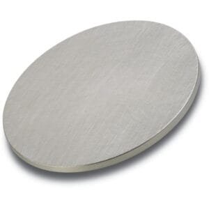
Cadmium Arsenide Sputtering Target (Cd₃As₂) is a specialized compound semiconductor material widely used in advanced condensed-matter physics and next-generation electronic research. As a prototypical three-dimensional Dirac semimetal, Cd₃As₂ exhibits ultra-high carrier mobility, linear energy dispersion, and unique quantum transport behavior. High-quality sputtering targets enable controlled thin-film deposition of Cd₃As₂ for both fundamental studies and emerging device concepts.
Detailed Description
Cd₃As₂ sputtering targets are manufactured from high-purity cadmium and arsenic precursors with precise stoichiometric control to ensure the correct Cd:As ratio. Advanced synthesis and ceramic consolidation processes—including controlled atmosphere processing, pressing, and densification—are used to achieve high density, uniform microstructure, and stable sputtering behavior.
Using a compound Cd₃As₂ target allows direct deposition of cadmium arsenide films without relying on complex co-sputtering or reactive gas balancing. This improves compositional consistency, reduces process variability, and enhances repeatability across deposition runs. Due to its semiconducting nature, Cd₃As₂ targets are typically operated under RF sputtering, providing stable plasma coupling and uniform erosion.
Thin films deposited from Cd₃As₂ sputtering targets are suitable for subsequent crystallization or epitaxial optimization through post-deposition annealing, depending on substrate selection and research objectives.
Applications
Cadmium Arsenide sputtering targets are primarily used in:
Topological materials research: Dirac and Weyl semimetal thin films
Quantum transport studies: High-mobility electronic systems
Advanced semiconductor research: Novel electronic and optoelectronic devices
Infrared and terahertz technologies: Functional semimetal films
Spintronics & quantum materials: Exploration of exotic electronic states
Academic & national laboratory R&D: Fundamental physics and materials science
Technical Parameters
| Parameter | Typical Value / Range | Importance |
|---|---|---|
| Chemical Composition | Cd₃As₂ | Defines Dirac semimetal behavior |
| Purity | 99.9% – 99.99% | Reduces impurity-induced scattering |
| Stoichiometry | Cd:As ≈ 3:2 | Ensures correct electronic structure |
| Diameter | 25 – 150 mm (custom) | Compatible with standard sputtering cathodes |
| Thickness | 3 – 6 mm (typical) | Influences target lifetime |
| Density | ≥ 95% of theoretical | Supports stable sputtering |
| Sputtering Mode | RF sputtering | Suitable for compound semiconductors |
| Bonding | Indium / Elastomer / Direct | Improves thermal stability |
Comparison with Related Semiconductor Targets
| Material | Key Advantage | Typical Application |
|---|---|---|
| Cd₃As₂ | 3D Dirac semimetal, ultra-high mobility | Quantum & topological research |
| CdTe | Direct bandgap semiconductor | Infrared & photovoltaic devices |
| HgCdTe | Tunable bandgap | IR detectors |
| Bi₂Se₃ | Topological insulator | Surface-state electronics |
FAQ
| Question | Answer |
|---|---|
| Can Cd₃As₂ sputtering targets be customized? | Yes, size, purity, density, and bonding can be tailored. |
| Which sputtering method is recommended? | RF sputtering is generally preferred for Cd₃As₂. |
| Are there safety considerations? | Yes, cadmium and arsenic compounds are handled under strict safety and compliance protocols. |
| How are the targets packaged? | Vacuum-sealed with protective cushioning for safe transport and storage. |
Packaging
Our Cadmium Arsenide Sputtering Targets (Cd₃As₂) are meticulously tagged and labeled to ensure traceability and strict quality control. Each target is vacuum-sealed and protected with reinforced cushioning to prevent contamination, oxidation, or mechanical damage during storage and transportation.
Conclusion
Cadmium Arsenide Sputtering Target (Cd₃As₂) provides a reliable platform for depositing high-quality Dirac semimetal thin films with controlled composition and reproducible performance. With precise stoichiometric control, stable sputtering behavior, and flexible customization options, Cd₃As₂ targets are ideally suited for advanced quantum materials research and emerging electronic applications.
For detailed specifications and a quotation, please contact us at sales@thinfilmmaterials.com.


Reviews
There are no reviews yet.