
CIGS Copper Indium Gallium Selenide Sputtering Target Description
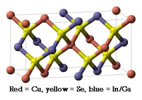
Copper Indium Gallium Selenide (CIGS) is a semiconductor material composed of copper, indium, gallium, and selenium. CIGS is characterized by its tetrahedrally bonded structure with a chalcopyrite crystal formation. CIGS sputtering targets are utilized in the production of solar thin-film batteries, which offer advantages such as low mass, extremely thin thickness, and flexibility. These properties make CIGS an ideal material for various advanced solar energy applications.
Copper
Copper is a chemical element with the symbol “Cu” and an atomic number of 29. The name “copper” originates from the Old English word ‘coper,’ which in turn is derived from the Latin term ‘Cyprium aes,’ meaning metal from Cyprus. Copper has been used since 9000 BC and was discovered by people from the Middle East. It is located in Period 4 and Group 11 of the periodic table, belonging to the d-block elements. The relative atomic mass of copper is approximately 63.546 Daltons, with the number in parentheses indicating a margin of uncertainty.
Related Product: Copper (Cu) Sputtering Target
Indium
Indium is a chemical element with the symbol “In” and an atomic number of 49. The name “indium” comes from the Latin word ‘indicium,’ meaning violet or indigo, referring to the indigo spectral line. It was first mentioned in 1863 and observed by Ferdinand Reich and Theodor Richter. The isolation of indium was later accomplished and announced by Theodor Richter. Indium is located in Period 5 and Group 13 of the periodic table, belonging to the p-block elements. Its relative atomic mass is approximately 114.818 Daltons, with the number in parentheses indicating a margin of uncertainty.
Related Product: Indium (In) Sputtering Target
Gallium
Gallium is a chemical element with the symbol “Ga” and an atomic number of 31. The name “gallium” originates from the Latin word ‘Gallia,’ meaning France. It was first mentioned in 1875 and observed by Paul-Émile Lecoq de Boisbaudran, who also accomplished and announced its isolation. Gallium is located in Period 4 and Group 13 of the periodic table, belonging to the p-block elements. Its relative atomic mass is approximately 69.723 Daltons, with the number in parentheses indicating a margin of uncertainty.
Selenium
Selenium is a chemical element with the symbol “Se” and an atomic number of 34. The name “selenium” is derived from the Greek word ‘selene,’ meaning moon. It was first mentioned in 1817 and observed by Jöns Jacob Berzelius and Johan Gottlieb Gahn, who also achieved and announced its isolation. Selenium is located in Period 4 and Group 16 of the periodic table, classified within the p-block elements. Its relative atomic mass is approximately 78.96 Daltons, with the number in parentheses indicating a margin of uncertainty.
Related Product: Selenium (Se) Sputtering Target
CIGS Copper Indium Gallium Selenide Sputtering Target Specification
| Compound Formula | CuInxGa(1-x)Se2 |
| Appearance | Silvery |
| Density | 5.7 g/cm3 |
| Melting Point | 990-1070 °C |
| Available Sizes | Dia.: 1.0″, 2.0″, 3.0″, 4.0″, 5.0″, 6.0″ Thick: 0.125″, 0.250″ |
CIGS Copper Indium Gallium Selenide Sputtering Target Application
The Copper Indium Gallium Selenide (CIGS) Sputtering Target is utilized in a variety of applications, including thin film deposition and decorative coatings. It is widely used in the semiconductor industry, display technologies, and the production of LEDs and photovoltaic devices. Additionally, this material is important for functional coatings, optical information storage, glass coating applications for automotive and architectural glass, and optical communication technologies.
CIGS Copper Indium Gallium Selenide Sputtering Target Packing
Our Copper Indium Gallium Selenide (CIGS) Sputtering Targets are meticulously tagged and labeled on the exterior to ensure efficient identification and maintain high quality control standards. We take extensive precautions to prevent any potential damage during storage and transportation, ensuring the targets arrive in perfect condition.


Reviews
There are no reviews yet.